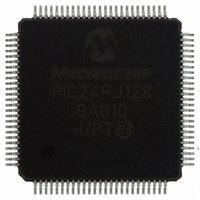
PIC24FJ128GA010-I/PT Microchip Technology, PIC24FJ128GA010-I/PT Datasheet - Page 101

PIC24FJ128GA010-I/PT
Manufacturer Part Number
PIC24FJ128GA010-I/PT
Description
IC PIC MCU FLASH 128K 100TQFP
Manufacturer
Microchip Technology
Series
PIC® 24Fr
Datasheets
1.PIC24FJ16GA002-ISS.pdf
(52 pages)
2.PIC24FJ64GA006-IPT.pdf
(240 pages)
3.PIC24FJ64GA006-IPT.pdf
(22 pages)
4.PIC24FJ128GA008-IPT.pdf
(12 pages)
5.PIC24FJ128GA006-IPT.pdf
(231 pages)
6.PIC24FJ128GA010-IPT.pdf
(230 pages)
Specifications of PIC24FJ128GA010-I/PT
Core Size
16-Bit
Program Memory Size
128KB (43K x 24)
Core Processor
PIC
Speed
16MHz
Connectivity
I²C, PMP, SPI, UART/USART
Peripherals
Brown-out Detect/Reset, POR, PWM, WDT
Number Of I /o
84
Program Memory Type
FLASH
Ram Size
8K x 8
Voltage - Supply (vcc/vdd)
2 V ~ 3.6 V
Data Converters
A/D 16x10b
Oscillator Type
Internal
Operating Temperature
-40°C ~ 85°C
Package / Case
100-TFQFP
Controller Family/series
PIC24
No. Of I/o's
84
Ram Memory Size
8KB
Cpu Speed
32MHz
No. Of Timers
5
No. Of Pwm Channels
5
Embedded Interface Type
EUART, I2C, PSP, SPI
Rohs Compliant
Yes
Processor Series
PIC24FJ
Core
PIC
Data Bus Width
16 bit
Data Ram Size
8 KB
Interface Type
SPI, I2C, USART
Maximum Clock Frequency
16 MHz
Number Of Programmable I/os
54
Number Of Timers
5
Maximum Operating Temperature
+ 85 C
Mounting Style
SMD/SMT
3rd Party Development Tools
52713-733, 52714-737, 53276-922, EWDSPIC
Development Tools By Supplier
PG164130, DV164035, DV244005, DV164005, PG164120, DM240001, DM240011
Minimum Operating Temperature
- 40 C
On-chip Adc
10 bit, 16 Channel
Package
100TQFP
Device Core
PIC
Family Name
PIC24
Maximum Speed
16 MHz
Operating Supply Voltage
2.5|3.3 V
Lead Free Status / RoHS Status
Lead free / RoHS Compliant
For Use With
DM240011 - KIT STARTER MPLAB FOR PIC24F MCUAC164333 - MODULE SKT FOR PM3 100QFPDV164033 - KIT START EXPLORER 16 MPLAB ICD2MA160011 - DAUGHTER BOARD PICDEM LCD 16F91XDM240001 - BOARD DEMO PIC24/DSPIC33/PIC32
Eeprom Size
-
Lead Free Status / Rohs Status
Details
Available stocks
Company
Part Number
Manufacturer
Quantity
Price
Company:
Part Number:
PIC24FJ128GA010-I/PT
Manufacturer:
Microchi
Quantity:
627
Company:
Part Number:
PIC24FJ128GA010-I/PT
Manufacturer:
MICROCHIP
Quantity:
212
Company:
Part Number:
PIC24FJ128GA010-I/PT
Manufacturer:
Microchip Technology
Quantity:
10 000
9.0
All of the device pins (except V
OSC1/CLKI) are shared between the peripherals and
the parallel I/O ports. All I/O input ports feature Schmitt
Trigger inputs for improved noise immunity.
9.1
A parallel I/O port that shares a pin with a peripheral is,
in general, subservient to the peripheral. The periph-
eral’s output buffer data and control signals are
provided to a pair of multiplexers. The multiplexers
select whether the peripheral or the associated port
has ownership of the output data and control signals of
the I/O pin. The logic also prevents “loop through”, in
which a port’s digital output can drive the input of a
peripheral that shares the same pin. Figure 9-1 shows
how ports are shared with other peripherals and the
associated I/O pin to which they are connected.
FIGURE 9-1:
© 2005 Microchip Technology Inc.
Note:
I/O PORTS
Parallel I/O (PIO) Ports
This data sheet summarizes the features
of this group of PIC24FJ devices. It is not
intended to be a comprehensive reference
source.
Read Port
Read LAT
Read TRIS
Data Bus
WR TRIS
WR LAT +
WR Port
BLOCK DIAGRAM OF A TYPICAL SHARED PORT STRUCTURE
Peripheral Output Enable
Peripheral Output Data
Peripheral Input Data
Peripheral Module Enable
Peripheral Module
PIO Module
DD
TRIS Latch
Data Latch
D
D
CK
CK
, V
SS
Q
Q
, MCLR and
Advance Information
Output Multiplexers
PIC24FJ128GA FAMILY
When a peripheral is enabled and the peripheral is
actively driving an associated pin, the use of the pin as
a general purpose output pin is disabled. The I/O pin
may be read, but the output driver for the parallel port
bit will be disabled. If a peripheral is enabled, but the
peripheral is not actively driving a pin, that pin may be
driven by a port.
All port pins have three registers directly associated
with their operation as digital I/O. The data direction
register (TRISx) determines whether the pin is an input
or an output. If the data direction bit is a ‘1’, then the pin
is an input. All port pins are defined as inputs after a
Reset. Reads from the latch (LATx), read the latch.
Writes to the latch, write the latch. Reads from the port
(PORTx), read the port pins, while writes to the port
pins, write the latch.
Any bit and its associated data and control registers
that are not valid for a particular device will be
disabled. That means the corresponding LATx and
TRISx registers and the port pin will read as zeros.
When a pin is shared with another peripheral or func-
tion that is defined as an input only, it is nevertheless
regarded as a dedicated port because there is no
other competing source of outputs. An example is the
INT4 pin.
1
0
1
0
Output Enable
Output Data
Input Data
I/O
I/O Pin
DS39747A-page 99


