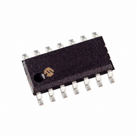
PIC16F506-I/SL Microchip Technology, PIC16F506-I/SL Datasheet - Page 90

PIC16F506-I/SL
Manufacturer Part Number
PIC16F506-I/SL
Description
IC PIC MCU FLASH 1KX14 14SOIC
Manufacturer
Microchip Technology
Series
PIC® 16Fr
Datasheets
1.PIC12F510-ISN.pdf
(124 pages)
2.PIC16F506-ISL.pdf
(12 pages)
3.PIC16F506-ISL.pdf
(8 pages)
4.PIC16F506-ISL.pdf
(22 pages)
5.PIC16F506-IP.pdf
(114 pages)
Specifications of PIC16F506-I/SL
Program Memory Type
FLASH
Program Memory Size
1.5KB (1K x 12)
Package / Case
14-SOIC (3.9mm Width), 14-SOL
Core Processor
PIC
Core Size
8-Bit
Speed
20MHz
Peripherals
POR, WDT
Number Of I /o
11
Ram Size
67 x 8
Voltage - Supply (vcc/vdd)
2 V ~ 5.5 V
Data Converters
A/D 4x8b
Oscillator Type
Internal
Operating Temperature
-40°C ~ 85°C
Processor Series
PIC16F
Core
PIC
Data Bus Width
8 bit
Data Ram Size
67 B
Maximum Clock Frequency
20 MHz
Number Of Programmable I/os
12
Number Of Timers
1
Maximum Operating Temperature
+ 85 C
Mounting Style
SMD/SMT
3rd Party Development Tools
52715-96, 52716-328, 52717-734
Development Tools By Supplier
PG164130, DV164035, DV244005, DV164005, PG164120, ICE2000
Minimum Operating Temperature
- 40 C
On-chip Adc
3-ch x 8-bit
Lead Free Status / RoHS Status
Lead free / RoHS Compliant
Eeprom Size
-
Connectivity
-
Lead Free Status / Rohs Status
Lead free / RoHS Compliant
Available stocks
Company
Part Number
Manufacturer
Quantity
Price
Company:
Part Number:
PIC16F506-I/SL
Manufacturer:
MICROCHIP
Quantity:
16 700
Company:
Part Number:
PIC16F506-I/SL
Manufacturer:
Microchip Technology
Quantity:
33 360
Part Number:
PIC16F506-I/SL
Manufacturer:
MICROCHIP/微芯
Quantity:
20 000
PIC12F510/16F506
13.3
DS41268D-page 88
DC CHARACTERISTICS
D030
D030A
D031
D032
D033
D033
D033
D040
D040A
D041
D042
D043
D043
D043
D070
D060
D062
D061A
D063
D080
D080A
D083
D083A
D090
D090A
D092
D092A
D100
D101
Note
Param
No.
1:
2:
3:
4:
5:
†
V
V
C
C
DC Characteristics: PIC12F510/16F506 (Industrial, Extended)
Sym
I
OL
OH
OSC
IO
V
V
PUR
I
IL
IH
IL
Data in “Typ” column is at 5V, 25°C unless otherwise stated. These parameters are for design guidance only and are not tested.
In EXTRC oscillator configuration, the OSC1/CLKIN pin is a Schmitt Trigger input. It is not recommended that the PIC12F510/16F506 be
driven with external clock in RC mode.
The leakage current on the MCLR pin is strongly dependent on the applied voltage level. The specified levels represent normal operating
conditions. Higher leakage current may be measured at different input voltages.
Negative current is defined as coming out of the pin.
This specification applies when GP3/MCLR is configured as an input with the pull-up disabled. The leakage current for the GP3/RB3/
MCLR pin is higher than for the standard I/O port pins.
This specification applies when GP3/RB3/MCLR is configured as the MCLR Reset pin function with the weak pull-up always enabled.
2 OSC2 pin
Input Low Voltage
I/O ports
with TTL buffer
with Schmitt Trigger buffer
MCLR, T0CKI
OSC1 (in EXTRC), EC
OSC1 (in HS)
OSC1 (in XT and LP)
Input High Voltage
I/O ports
with TTL buffer
with Schmitt Trigger buffer
MCLR, T0CKI
OSC1 (in EXTRC), EC
OSC1 (in HS)
OSC1 (in XT and LP)
GPIO/PORTB Weak Pull-up Current
Input Leakage Current
I/O ports
GP3/RB3/MCLR
GP3/RB3/MCLR
OSC1
Output Low Voltage
I/O ports/CLKOUT
OSC2
Output High Voltage
I/O ports/CLKOUT
OSC2
Capacitive Loading Specs on Output Pins
All I/O pins
Characteristic
(5)
(4)
(3)
(1)
(1)
(2), (3)
Standard Operating Conditions (unless otherwise specified)
Operating Temperature
V
V
V
V
0.25 V
0.85 V
0.85 V
0.85 V
0.7 V
+ 0.8V
DD
DD
DD
DD
Min
V
V
V
V
V
V
V
2.0
1.6
50
—
50
—
—
—
—
—
—
—
—
SS
SS
SS
SS
SS
SS
SS
– 0.7
– 0.7
– 0.7
– 0.7
DD
DD
DD
DD
DD
Typ†
+0.7
250
250
—
—
—
—
—
—
—
—
—
—
—
—
—
—
—
—
—
—
—
—
—
—
—
—
—
—
—
0.15 V
0.15 V
0.15 V
0.15 V
0.3 V
0.3 V
0.8V
Max
V
V
V
V
V
V
V
400
400
0.6
0.6
0.6
0.6
±1
±5
±5
—
—
—
—
15
50
DD
DD
DD
DD
DD
DD
DD
DD
DD
DD
DD
DD
DD
-40°C ≤ T
-40°C ≤ T
Units
μA
μA
μA
μA
μA
pF
pF
V
V
V
V
V
V
V
V
V
V
V
V
V
V
V
V
V
V
V
V
V
V
A
A
≤ +85°C (industrial)
≤ +125°C (extended)
For 4.5 ≤ V
otherwise
4.5 ≤ V
Otherwise
For entire V
V
V
V
V
V
configuration
I
I
I
I
I
I
I
I
In XT, HS and LP modes when external clock
is used to drive OSC1.
OL
OL
OL
OL
OH
OH
OH
OH
DD
SS
DD
SS
SS
= 8.5 mA, V
= 7.0 mA, V
= 1.6 mA, V
= 1.2 mA, V
= -3.0 mA, V
= -2.5 mA, V
= -1.3 mA, V
= -1.0 mA, V
≤ V
≤ V
≤ V
= 5V, V
= 5V
© 2007 Microchip Technology Inc.
DD
PIN
PIN
PIN
≤ 5.5V
DD
≤ V
≤ V
≤ V
DD
PIN
≤ 5.5V
DD
DD
DD
range
= V
DD
DD
DD
DD
Conditions
DD
DD
DD
DD
, Pin at high-impedance
, XT, HS and LP oscillator
= 4.5V, –40°C to +85°C
= 4.5V, –40°C to +125°C
= 4.5V, –40°C to +85°C
= 4.5V, –40°C to +125°C
SS
= 4.5V, –40°C to +85°C
= 4.5V, –40°C to +125°C
= 4.5V, –40°C to +85°C
= 4.5V, –40°C to +125°C


