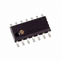
PIC16F506-I/SL Microchip Technology, PIC16F506-I/SL Datasheet - Page 51

PIC16F506-I/SL
Manufacturer Part Number
PIC16F506-I/SL
Description
IC PIC MCU FLASH 1KX14 14SOIC
Manufacturer
Microchip Technology
Series
PIC® 16Fr
Datasheets
1.PIC12F510-ISN.pdf
(124 pages)
2.PIC16F506-ISL.pdf
(12 pages)
3.PIC16F506-ISL.pdf
(8 pages)
4.PIC16F506-ISL.pdf
(22 pages)
5.PIC16F506-IP.pdf
(114 pages)
Specifications of PIC16F506-I/SL
Program Memory Type
FLASH
Program Memory Size
1.5KB (1K x 12)
Package / Case
14-SOIC (3.9mm Width), 14-SOL
Core Processor
PIC
Core Size
8-Bit
Speed
20MHz
Peripherals
POR, WDT
Number Of I /o
11
Ram Size
67 x 8
Voltage - Supply (vcc/vdd)
2 V ~ 5.5 V
Data Converters
A/D 4x8b
Oscillator Type
Internal
Operating Temperature
-40°C ~ 85°C
Processor Series
PIC16F
Core
PIC
Data Bus Width
8 bit
Data Ram Size
67 B
Maximum Clock Frequency
20 MHz
Number Of Programmable I/os
12
Number Of Timers
1
Maximum Operating Temperature
+ 85 C
Mounting Style
SMD/SMT
3rd Party Development Tools
52715-96, 52716-328, 52717-734
Development Tools By Supplier
PG164130, DV164035, DV244005, DV164005, PG164120, ICE2000
Minimum Operating Temperature
- 40 C
On-chip Adc
3-ch x 8-bit
Lead Free Status / RoHS Status
Lead free / RoHS Compliant
Eeprom Size
-
Connectivity
-
Lead Free Status / Rohs Status
Lead free / RoHS Compliant
Available stocks
Company
Part Number
Manufacturer
Quantity
Price
Company:
Part Number:
PIC16F506-I/SL
Manufacturer:
MICROCHIP
Quantity:
16 700
Company:
Part Number:
PIC16F506-I/SL
Manufacturer:
Microchip Technology
Quantity:
33 360
Part Number:
PIC16F506-I/SL
Manufacturer:
MICROCHIP/微芯
Quantity:
20 000
8.0
The comparator voltage reference module also allows
the selection of an internally generated voltage refer-
ence for one of the C2 comparator inputs. The VRCON
register (Register 8-1) controls the voltage reference
module shown in Figure 8-1.
8.1
The voltage reference can output 32 voltage levels; 16
in a high range and 16 in a low range.
Equation 8-1 determines the output voltages:
EQUATION 8-1:
REGISTER 8-1:
© 2007 Microchip Technology Inc.
bit 7
Legend:
R = Readable bit
-n = Value at POR
bit 7
bit 6
bit 5
bit 4
bit 3-0
Note 1:
VRR = 0 (high range):
VRR = 1 (low range): CV
R/W-0
VREN
2:
CV
COMPARATOR VOLTAGE
REFERENCE MODULE
(PIC16F506 ONLY)
Configuring The Voltage
Reference
REF
When this bit is set, the TRIS for the CV
CV
CV
= (V
REF
REF
VREN: CV
1 = CV
0 = CV
VROE: CV
1 = CV
0 = CV
VRR: CV
1 = Low range
0 = High range
Unimplemented: Read as ‘1’
VR<3:0> CV
When V
When V
DD
pin.
controls for ratio metric reference applies to Comparator 2 on the PIC16F506 only.
R/W-0
VROE
/4) + (VR<3:0> x V
VRCON: VOLTAGE REFERENCE CONTROL REGISTER (PIC16F506 ONLY)
REF
REF
REF
REF
RR
RR
REF
REF
REF
REF
= 1: CV
= 0: CV
is powered on
is powered down, no current is drawn
output is enabled
output is disabled
= (VR<3:0>/24) x V
REF
Range Selection bit
W = Writable bit
‘1’ = Bit is set
Enable bit
Output Enable bit
Value Selection bit
R/W-1
VRR
REF
REF
= (VR<3:0>/24)*V
= V
DD
/32)
DD
/4+(VR<3:0>/32)*V
DD
(1)
U-1
—
REF
pin is overridden and the analog voltage is placed on the
DD
U = Unimplemented bit, read as ‘0’, except if denoted
otherwise
‘0’ = Bit is cleared
R/W-1
8.2
The full range of V
construction of the module. The transistors on the top
and bottom of the resistor ladder network (Figure 8-1)
keep CV
tion is when the module is disabled by clearing the
VREN bit (VRCON<7>). When disabled, the reference
voltage is V
(VRCON<5>) bit is set. This allows the comparator to
detect a zero-crossing and not consume the CV
module current.
The voltage reference is V
the CV
tested absolute accuracy of the comparator voltage
reference can be found in Section 13.2 “DC Charac-
teristics: PIC12F510/16F506 (Extended)”.
VR3
DD
PIC12F510/16F506
REF
REF
Voltage Reference Accuracy/Error
output changes with fluctuations in V
SS
from approaching V
R/W-1
VR2
when VR<3:0> is ‘0000’ and the VRR
SS
to V
DD
x = Bit is unknown
DD
cannot be realized due to
R/W-1
VR1
derived and, therefore,
SS
or V
DS41268D-page 49
DD
. The excep-
R/W-1
VR0
DD
. The
bit 0
REF


