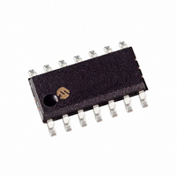
PIC16F506-I/SL Microchip Technology, PIC16F506-I/SL Datasheet - Page 16

PIC16F506-I/SL
Manufacturer Part Number
PIC16F506-I/SL
Description
IC PIC MCU FLASH 1KX14 14SOIC
Manufacturer
Microchip Technology
Series
PIC® 16Fr
Datasheets
1.PIC12F510-ISN.pdf
(124 pages)
2.PIC16F506-ISL.pdf
(12 pages)
3.PIC16F506-ISL.pdf
(8 pages)
4.PIC16F506-ISL.pdf
(22 pages)
5.PIC16F506-IP.pdf
(114 pages)
Specifications of PIC16F506-I/SL
Program Memory Type
FLASH
Program Memory Size
1.5KB (1K x 12)
Package / Case
14-SOIC (3.9mm Width), 14-SOL
Core Processor
PIC
Core Size
8-Bit
Speed
20MHz
Peripherals
POR, WDT
Number Of I /o
11
Ram Size
67 x 8
Voltage - Supply (vcc/vdd)
2 V ~ 5.5 V
Data Converters
A/D 4x8b
Oscillator Type
Internal
Operating Temperature
-40°C ~ 85°C
Processor Series
PIC16F
Core
PIC
Data Bus Width
8 bit
Data Ram Size
67 B
Maximum Clock Frequency
20 MHz
Number Of Programmable I/os
12
Number Of Timers
1
Maximum Operating Temperature
+ 85 C
Mounting Style
SMD/SMT
3rd Party Development Tools
52715-96, 52716-328, 52717-734
Development Tools By Supplier
PG164130, DV164035, DV244005, DV164005, PG164120, ICE2000
Minimum Operating Temperature
- 40 C
On-chip Adc
3-ch x 8-bit
Lead Free Status / RoHS Status
Lead free / RoHS Compliant
Eeprom Size
-
Connectivity
-
Lead Free Status / Rohs Status
Lead free / RoHS Compliant
Available stocks
Company
Part Number
Manufacturer
Quantity
Price
Company:
Part Number:
PIC16F506-I/SL
Manufacturer:
MICROCHIP
Quantity:
16 700
Company:
Part Number:
PIC16F506-I/SL
Manufacturer:
Microchip Technology
Quantity:
33 360
Part Number:
PIC16F506-I/SL
Manufacturer:
MICROCHIP/微芯
Quantity:
20 000
PIC12F510/16F506
3.1
The clock input (OSC1/CLKIN pin) is internally divided
by four to generate four non-overlapping quadrature
clocks, namely Q1, Q2, Q3 and Q4. Internally, the PC
is incremented every Q1 and the instruction is fetched
from program memory and latched into the instruction
register in Q4. It is decoded and executed during the
following Q1 through Q4. The clocks and instruction
execution flow is shown in Figure 3-3 and Example 3-1.
FIGURE 3-3:
EXAMPLE 3-1:
DS41268D-page 14
1. MOVLW 03H
2. MOVWF PORTB
3. CALL SUB_1
4. BSF PORTB, BIT1
All instructions are single cycle, except for any program branches. These take two cycles, since the fetch instruction
is “flushed” from the pipeline, while the new instruction is being fetched and then executed.
Clocking Scheme/Instruction
Cycle
OSC1
PC
Q1
Q2
Q3
Q4
CLOCK/INSTRUCTION CYCLE
INSTRUCTION PIPELINE FLOW
Q1
Execute INST (PC – 1)
Fetch INST (PC)
Q2
Fetch 1
PC
Q3
Execute 1
Q4
Fetch 2
Q1
Execute INST (PC)
Fetch INST (PC + 1)
Execute 2
Q2
Fetch 3
PC + 1
3.2
An instruction cycle consists of four Q cycles (Q1, Q2,
Q3 and Q4). The instruction fetch and execute are
pipelined such that fetch takes one instruction cycle,
while decode and execute take another instruction
cycle. However, due to the pipelining, each instruction
effectively executes in one cycle. If an instruction
causes the PC to change (e.g., GOTO), then two cycles
are required to complete the instruction (Example 3-1).
A fetch cycle begins with the PC incrementing in Q1.
In the execution cycle, the fetched instruction is latched
into the Instruction Register (IR) in cycle Q1. This
instruction is then decoded and executed during the
Q2, Q3 and Q4 cycles. Data memory is read during Q2
(operand read) and written during Q4 (destination
write).
Q3
Execute 3
Q4
Fetch 4
Instruction Flow/Pipelining
Q1
Fetch SUB_1 Execute SUB_1
Execute INST (PC + 1)
Fetch INST (PC + 2)
Q2
Flush
© 2007 Microchip Technology Inc.
PC + 2
Q3
Q4
Internal
Phase
Clock


