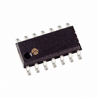
PIC16F506-I/SL Microchip Technology, PIC16F506-I/SL Datasheet - Page 23

PIC16F506-I/SL
Manufacturer Part Number
PIC16F506-I/SL
Description
IC PIC MCU FLASH 1KX14 14SOIC
Manufacturer
Microchip Technology
Series
PIC® 16Fr
Datasheets
1.PIC12F510-ISN.pdf
(124 pages)
2.PIC16F506-ISL.pdf
(12 pages)
3.PIC16F506-ISL.pdf
(8 pages)
4.PIC16F506-ISL.pdf
(22 pages)
5.PIC16F506-IP.pdf
(114 pages)
Specifications of PIC16F506-I/SL
Program Memory Type
FLASH
Program Memory Size
1.5KB (1K x 12)
Package / Case
14-SOIC (3.9mm Width), 14-SOL
Core Processor
PIC
Core Size
8-Bit
Speed
20MHz
Peripherals
POR, WDT
Number Of I /o
11
Ram Size
67 x 8
Voltage - Supply (vcc/vdd)
2 V ~ 5.5 V
Data Converters
A/D 4x8b
Oscillator Type
Internal
Operating Temperature
-40°C ~ 85°C
Processor Series
PIC16F
Core
PIC
Data Bus Width
8 bit
Data Ram Size
67 B
Maximum Clock Frequency
20 MHz
Number Of Programmable I/os
12
Number Of Timers
1
Maximum Operating Temperature
+ 85 C
Mounting Style
SMD/SMT
3rd Party Development Tools
52715-96, 52716-328, 52717-734
Development Tools By Supplier
PG164130, DV164035, DV244005, DV164005, PG164120, ICE2000
Minimum Operating Temperature
- 40 C
On-chip Adc
3-ch x 8-bit
Lead Free Status / RoHS Status
Lead free / RoHS Compliant
Eeprom Size
-
Connectivity
-
Lead Free Status / Rohs Status
Lead free / RoHS Compliant
Available stocks
Company
Part Number
Manufacturer
Quantity
Price
Company:
Part Number:
PIC16F506-I/SL
Manufacturer:
MICROCHIP
Quantity:
16 700
Company:
Part Number:
PIC16F506-I/SL
Manufacturer:
Microchip Technology
Quantity:
33 360
Part Number:
PIC16F506-I/SL
Manufacturer:
MICROCHIP/微芯
Quantity:
20 000
4.4
The OPTION register is a 8-bit wide, write-only register,
that contains various control bits to configure the
Timer0/WDT prescaler and Timer0.
By executing the OPTION instruction, the contents of
the W register will be transferred to the OPTION
register. A Reset sets the OPTION<7:0> bits.
REGISTER 4-3:
© 2007 Microchip Technology Inc.
bit 7
Legend:
R = Readable bit
-n = Value at POR
bit 7
bit 6
bit 5
bit 4
bit 3
bit 2-0
Note 1: If TRIS bit is set to ‘0’, the wake-up on
GPWU
W-1
2: If the T0CS bit is set to ‘1’, it will override
OPTION Register
change
disabled for that pin (i.e., note that TRIS
overrides Option control of GPPU/RBPU
and GPWU/RBWU).
the TRIS function on the T0CKI pin.
GPWU: Enable Wake-up On Pin Change bit (GP0, GP1, GP3)
1 = Disabled
0 = Enabled
GPPU: Enable Weak Pull-Ups bit (GP0, GP1, GP3)
1 = Disabled
0 = Enabled
T0CS: Timer0 Clock Source Select bit
1 = Transition on T0CKI pin
0 = Internal instruction cycle clock (CLKOUT)
T0SE: Timer0 Source Edge Select bit
1 = Increment on high-to-low transition on T0CKI pin
0 = Increment on low-to-high transition on T0CKI pin
PSA: Prescaler Assignment bit
1 = Prescaler assigned to the WDT
0 = Prescaler assigned to Timer0
PS<2:0>: Prescaler Rate Select bits
GPPU
W-1
and
OPTION_REG: OPTION REGISTER (PIC12F510)
Bit Value
pull-up
000
001
010
011
100
101
110
111
W = Writable bit
‘1’ = Bit is set
T0CS
W-1
Timer0 Rate
functions
1 : 2
1 : 4
1 : 8
1 : 16
1 : 32
1 : 64
1 : 128
1 : 256
T0SE
W-1
are
WDT Rate
1 : 1
1 : 2
1 : 4
1 : 8
1 : 16
1 : 32
1 : 64
1 : 128
U = Unimplemented bit, read as ‘0’
‘0’ = Bit is cleared
W-1
PSA
PIC12F510/16F506
W-1
PS2
x = Bit is unknown
W-1
PS1
DS41268D-page 21
W-1
PS0
bit 0


