CDB4265 Cirrus Logic Inc, CDB4265 Datasheet - Page 4
CDB4265
Manufacturer Part Number
CDB4265
Description
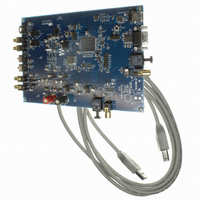
BOARD EVAL FOR CS4265 CODEC
Manufacturer
Cirrus Logic Inc
Specifications of CDB4265
Main Purpose
Audio, CODEC
Embedded
No
Utilized Ic / Part
CS4265
Primary Attributes
Stereo, 24-Bit, 192 kHz Sample Rate
Secondary Attributes
Graphic User Interface, S/PDIF/ I2S / I2C / SPI Interface
Description/function
Audio CODECs
Operating Supply Voltage
5 V
Product
Audio Modules
For Use With/related Products
CS4265
Lead Free Status / RoHS Status
Contains lead / RoHS non-compliant
Lead Free Status / RoHS Status
Lead free / RoHS Compliant, Contains lead / RoHS non-compliant
Other names
598-1001


4
7. PARAMETER DEFINITIONS ................................................................................................................ 46
8. DAC FILTER PLOTS
9. ADC FILTER PLOTS
10. EXTERNAL IEC60958-3 TRANSMITTER COMPONENTS ............................................................... 51
11. CHANNEL STATUS BUFFER MANAGEMENT ................................................................................ 52
6.4 ADC Control - Address 04h ............................................................................................................ 37
6.5 MCLK Frequency - Address 05h .................................................................................................... 38
6.6 Signal Selection - Address 06h ...................................................................................................... 39
6.7 Channel B PGA Control - Address 07h .......................................................................................... 39
6.8 Channel A PGA Control - Address 08h .......................................................................................... 39
6.9 ADC Input Control - Address 09h ................................................................................................... 40
6.10 DAC Channel A Volume Control - Address 0Ah ........................................................................... 40
6.11 DAC Channel B Volume Control - Address 0Bh ........................................................................... 41
6.12 DAC Control 2 - Address 0Ch ...................................................................................................... 41
6.13 Status - Address 0Dh ................................................................................................................... 42
6.14 Status Mask - Address 0Eh .......................................................................................................... 43
6.15 Status Mode MSB - Address 0Fh ................................................................................................. 43
6.16 Status Mode LSB - Address 10h .................................................................................................. 43
6.17 Transmitter Control 1 - Address 11h ............................................................................................ 43
6.18 Transmitter Control 2 - Address 12h ............................................................................................ 44
10.1 IEC60958-3 Transmitter External Components ............................................................................ 51
10.2 Isolating Transformer Requirements ............................................................................................ 51
11.1 IEC60958-3 Channel Status (C) Bit Management ........................................................................ 52
6.3.1 DAC Digital Interface Format (Bits 5:4) ................................................................................. 36
6.3.2 Mute DAC (Bit 2) ................................................................................................................... 36
6.3.3 De-Emphasis Control (Bit 1) .................................................................................................. 37
6.4.1 Functional Mode (Bits 7:6) .................................................................................................... 37
6.4.2 ADC Digital Interface Format (Bit 4) ...................................................................................... 37
6.4.3 Mute ADC (Bit 2) ................................................................................................................... 38
6.4.4 ADC High-Pass Filter Freeze (Bit 1) ..................................................................................... 38
6.4.5 Master / Slave Mode (Bit 0) ................................................................................................... 38
6.5.1 Master Clock Dividers (Bits 6:4) ............................................................................................ 38
6.6.1 DAC SDIN Source (Bit 7) ...................................................................................................... 39
6.6.2 Digital Loopback (Bit 1) ......................................................................................................... 39
6.7.1 Channel B PGA Gain (Bits 5:0) ............................................................................................. 39
6.8.1 Channel A PGA Gain (Bits 5:0) ............................................................................................. 39
6.9.1 PGA Soft Ramp or Zero Cross Enable (Bits 4:3) .................................................................. 40
6.9.2 Analog Input Selection (Bit 0) ................................................................................................ 40
6.11.1 Volume Control (Bits 7:0) .................................................................................................... 41
6.12.1 DAC Soft Ramp or Zero Cross Enable (Bits 7:6) ................................................................ 41
6.12.2 Invert DAC Output (Bit 5) .................................................................................................... 42
6.13.1 E to F C-Buffer Transfer ...................................................................................................... 42
6.13.2 Clock Error (Bit 3) ................................................................................................................ 42
6.13.3 ADC Overflow (Bit 1) ........................................................................................................... 42
6.13.4 ADC Underflow (Bit 0) ......................................................................................................... 42
6.17.1 E to F C-Data Buffer Transfer Inhibit (Bit 6) ........................................................................ 43
6.17.2 C-Data Access Mode (Bit 5) ................................................................................................ 43
6.18.1 Transmitter Digital Interface Format (Bits 7:6) .................................................................... 44
6.18.2 Transmitter Output Driver Control (Bit 5) ............................................................................. 44
6.18.3 Transmitter Mute Control (Bit 4) .......................................................................................... 44
6.18.4 Transmitted Validity Bit Control (Bit 3) ................................................................................ 44
6.18.5 Transmitter Mono/Stereo Operation Control (Bit 2) ............................................................. 44
6.18.6 Mono Mode CS Data Source (Bit 1) .................................................................................... 44
6.18.7 Mono Mode Channel Selection (Bit 0) ................................................................................. 45
......................................................................................................................... 49
.................................................................................................................... 47
CS4265
DS657F2
Related parts for CDB4265
Image
Part Number
Description
Manufacturer
Datasheet
Request
R

Part Number:
Description:
Development Kit
Manufacturer:
Cirrus Logic Inc
Datasheet:
Part Number:
Description:
Development Kit
Manufacturer:
Cirrus Logic Inc
Datasheet:


Part Number:
Description:
High-efficiency PFC + Fluorescent Lamp Driver Reference Design
Manufacturer:
Cirrus Logic Inc
Datasheet:
Part Number:
Description:
Development Kit
Manufacturer:
Cirrus Logic Inc
Datasheet:
Part Number:
Description:
Development Kit
Manufacturer:
Cirrus Logic Inc
Datasheet:

Part Number:
Description:
Development Kit
Manufacturer:
Cirrus Logic Inc
Datasheet:
Part Number:
Description:
Development Kit
Manufacturer:
Cirrus Logic Inc
Datasheet:
Part Number:
Description:
Development Kit
Manufacturer:
Cirrus Logic Inc
Datasheet:
Part Number:
Description:
Development Kit
Manufacturer:
Cirrus Logic Inc
Datasheet:

Part Number:
Description:
EVALUATION BOARD FOR CS8427
Manufacturer:
Cirrus Logic Inc
Datasheet:

Part Number:
Description:
BOARD EVAL FOR CS8416 RCVR
Manufacturer:
Cirrus Logic Inc
Datasheet:

Part Number:
Description:
EVALUATION BOARD FOR CS8420
Manufacturer:
Cirrus Logic Inc
Datasheet:

Part Number:
Description:
KIT DEVELOPMENT EP9315 ARM9
Manufacturer:
Cirrus Logic Inc
Datasheet:

Part Number:
Description:
KIT DEVELOPMENT EP9302 ARM9
Manufacturer:
Cirrus Logic Inc
Datasheet: