CDB4265 Cirrus Logic Inc, CDB4265 Datasheet - Page 3
CDB4265
Manufacturer Part Number
CDB4265
Description
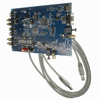
BOARD EVAL FOR CS4265 CODEC
Manufacturer
Cirrus Logic Inc
Specifications of CDB4265
Main Purpose
Audio, CODEC
Embedded
No
Utilized Ic / Part
CS4265
Primary Attributes
Stereo, 24-Bit, 192 kHz Sample Rate
Secondary Attributes
Graphic User Interface, S/PDIF/ I2S / I2C / SPI Interface
Description/function
Audio CODECs
Operating Supply Voltage
5 V
Product
Audio Modules
For Use With/related Products
CS4265
Lead Free Status / RoHS Status
Contains lead / RoHS non-compliant
Lead Free Status / RoHS Status
Lead free / RoHS Compliant, Contains lead / RoHS non-compliant
Other names
598-1001


DS657F2
TABLE OF CONTENTS
1. PIN DESCRIPTIONS
2. CHARACTERISTICS AND SPECIFICATIONS ...................................................................................... 9
3. TYPICAL CONNECTION DIAGRAM ................................................................................................... 23
4. APPLICATIONS ................................................................................................................................... 24
5. REGISTER QUICK REFERENCE ........................................................................................................ 33
6. REGISTER DESCRIPTION .................................................................................................................. 35
4.1 Recommended Power-Up Sequence ............................................................................................. 24
4.2 System Clocking ............................................................................................................................. 24
4.3 High-Pass Filter and DC Offset Calibration .................................................................................... 25
4.4 Analog Input Multiplexer, PGA, and Mic Gain ................................................................................ 26
4.5 Input Connections ........................................................................................................................... 26
4.6 Output Connections ........................................................................................................................ 27
4.7 Output Transient Control ................................................................................................................ 27
4.8 DAC Serial Data Input Multiplexer .................................................................................................. 28
4.9 De-Emphasis Filter ......................................................................................................................... 28
4.10 Internal Digital Loopback .............................................................................................................. 28
4.11 Mute Control ................................................................................................................................. 29
4.12 AES3 Transmitter ......................................................................................................................... 29
4.13 I²C Control Port Description and Timing ....................................................................................... 30
4.14 Status Reporting ........................................................................................................................... 31
4.15 Reset ............................................................................................................................................ 32
4.16 Synchronization of Multiple Devices ............................................................................................. 32
4.17 Grounding and Power Supply Decoupling .................................................................................... 32
4.18 Package Considerations ............................................................................................................... 32
6.1 Chip ID - Register 01h .................................................................................................................... 35
6.2 Power Control - Address 02h ......................................................................................................... 35
6.3 DAC Control - Address 03h ............................................................................................................ 36
SPECIFIED OPERATING CONDITIONS ............................................................................................. 9
ABSOLUTE MAXIMUM RATINGS ....................................................................................................... 9
DAC ANALOG CHARACTERISTICS ................................................................................................. 10
DAC COMBINED INTERPOLATION & ON-CHIP ANALOG FILTER RESPONSE ............................ 11
ADC ANALOG CHARACTERISTICS ................................................................................................. 13
ADC ANALOG CHARACTERISTICS ................................................................................................. 15
ADC DIGITAL FILTER CHARACTERISTICS ..................................................................................... 16
DC ELECTRICAL CHARACTERISTICS ............................................................................................. 17
DIGITAL INTERFACE CHARACTERISTICS ...................................................................................... 18
SWITCHING CHARACTERISTICS - SERIAL AUDIO PORT ............................................................. 19
SWITCHING CHARACTERISTICS - I²C CONTROL PORT ............................................................... 22
4.2.1 Master Clock ......................................................................................................................... 24
4.2.2 Master Mode ......................................................................................................................... 25
4.2.3 Slave Mode ........................................................................................................................... 25
4.5.1 Pseudo-Differential Input ....................................................................................................... 26
4.7.1 Power-Up .............................................................................................................................. 27
4.7.2 Power-Down .......................................................................................................................... 27
4.7.3 Serial Interface Clock Changes ............................................................................................. 27
4.12.1 TxOut Driver ........................................................................................................................ 29
4.12.2 Mono Mode Operation ......................................................................................................... 30
6.2.1 Freeze (Bit 7) ......................................................................................................................... 35
6.2.2 Power-Down MIC (Bit 3) ........................................................................................................ 35
6.2.3 Power-Down ADC (Bit 2) ....................................................................................................... 35
6.2.4 Power-Down DAC (Bit 1) ....................................................................................................... 36
6.2.5 Power-Down Device (Bit 0) ................................................................................................... 36
.......................................................................................................................... 7
CS4265
3
Related parts for CDB4265
Image
Part Number
Description
Manufacturer
Datasheet
Request
R

Part Number:
Description:
Development Kit
Manufacturer:
Cirrus Logic Inc
Datasheet:
Part Number:
Description:
Development Kit
Manufacturer:
Cirrus Logic Inc
Datasheet:


Part Number:
Description:
High-efficiency PFC + Fluorescent Lamp Driver Reference Design
Manufacturer:
Cirrus Logic Inc
Datasheet:
Part Number:
Description:
Development Kit
Manufacturer:
Cirrus Logic Inc
Datasheet:
Part Number:
Description:
Development Kit
Manufacturer:
Cirrus Logic Inc
Datasheet:

Part Number:
Description:
Development Kit
Manufacturer:
Cirrus Logic Inc
Datasheet:
Part Number:
Description:
Development Kit
Manufacturer:
Cirrus Logic Inc
Datasheet:
Part Number:
Description:
Development Kit
Manufacturer:
Cirrus Logic Inc
Datasheet:
Part Number:
Description:
Development Kit
Manufacturer:
Cirrus Logic Inc
Datasheet:

Part Number:
Description:
EVALUATION BOARD FOR CS8427
Manufacturer:
Cirrus Logic Inc
Datasheet:

Part Number:
Description:
BOARD EVAL FOR CS8416 RCVR
Manufacturer:
Cirrus Logic Inc
Datasheet:

Part Number:
Description:
EVALUATION BOARD FOR CS8420
Manufacturer:
Cirrus Logic Inc
Datasheet:

Part Number:
Description:
KIT DEVELOPMENT EP9315 ARM9
Manufacturer:
Cirrus Logic Inc
Datasheet:

Part Number:
Description:
KIT DEVELOPMENT EP9302 ARM9
Manufacturer:
Cirrus Logic Inc
Datasheet: