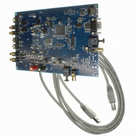
CDB4265 Cirrus Logic Inc, CDB4265 Datasheet - Page 26

CDB4265
Manufacturer Part Number
CDB4265
Description
BOARD EVAL FOR CS4265 CODEC
Manufacturer
Cirrus Logic Inc
Specifications of CDB4265
Main Purpose
Audio, CODEC
Embedded
No
Utilized Ic / Part
CS4265
Primary Attributes
Stereo, 24-Bit, 192 kHz Sample Rate
Secondary Attributes
Graphic User Interface, S/PDIF/ I2S / I2C / SPI Interface
Description/function
Audio CODECs
Operating Supply Voltage
5 V
Product
Audio Modules
For Use With/related Products
CS4265
Lead Free Status / RoHS Status
Contains lead / RoHS non-compliant
Lead Free Status / RoHS Status
Lead free / RoHS Compliant, Contains lead / RoHS non-compliant
Other names
598-1001
26
4.4
4.5
4.5.1
Analog Input Multiplexer, PGA, and Mic Gain
The CS4265 contains a stereo 2-to-1 analog input multiplexer followed by a programmable gain amplifier
(PGA). The input multiplexer is able to select either a line-level input source, or a mic-level input source, and
route it to the PGA. The mic-level input passes through a +32 dB gain stage prior to the input multiplexer,
allowing it to be used for microphone-level signals without the need for any external gain. The PGA stage
provides 12 dB of gain or attenuation in 0.5 dB steps.
plexer, PGA, and mic gain stages.
The
tiplexer and mic gain.
Address 08h” on page 39
level input is selected by the input multiplexer, and the PGA is set to 0 dB.
Input Connections
The analog modulator samples the input at 6.144 MHz (MCLK=12.288 MHz). The digital filter will reject sig-
nals within the stopband of the filter. However, there is no rejection for input signals which are
(n
for the recommended analog input circuit that will attenuate noise energy at 6.144 MHz. The use of capac-
itors which have a large voltage coefficient (such as general-purpose ceramics) must be avoided since
these can degrade signal linearity. Any unused analog input pairs should be left unconnected.
Pseudo-Differential Input
The CS4265 implements a pseudo-differential input stage. The SGND input is intended to be used as a
pseudo-differential reference signal. This feature allows for common mode noise rejection with single-
ended signals.
ferential input stage. The Typical Connection Diagram shows the recommended pseudo-differential input
×
““Analog Input Selection (Bit 0)” on page
6.144 MHz) the digital passband frequency, where n=0,1,2,... Refer to the Typical Connection Diagram
Figure 12
“Channel B PGA Control - Address 07h” on page 39
outline the register settings necessary to control the PGA. By default, the line-
MICIN1
MICIN2
shows a basic diagram outlining the internal implementation of the pseudo-dif-
AINA
AINB
Figure 11. Analog Input Architecture
+32 dB
+32 dB
Selection Bits
Analog Input
MUX
MUX
40” outlines the bit settings necessary to control the input mul-
PGA Gain Bits
PGA Gain Bits
Channel A
Channel B
PGA
PGA
Figure 11
Out to ADC
Channel B
Out to ADC
Channel A
shows the architecture of the input multi-
and
“Channel A PGA Control -
CS4265
DS657F2


