CDB4265 Cirrus Logic Inc, CDB4265 Datasheet - Page 27
CDB4265
Manufacturer Part Number
CDB4265
Description
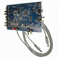
BOARD EVAL FOR CS4265 CODEC
Manufacturer
Cirrus Logic Inc
Specifications of CDB4265
Main Purpose
Audio, CODEC
Embedded
No
Utilized Ic / Part
CS4265
Primary Attributes
Stereo, 24-Bit, 192 kHz Sample Rate
Secondary Attributes
Graphic User Interface, S/PDIF/ I2S / I2C / SPI Interface
Description/function
Audio CODECs
Operating Supply Voltage
5 V
Product
Audio Modules
For Use With/related Products
CS4265
Lead Free Status / RoHS Status
Contains lead / RoHS non-compliant
Lead Free Status / RoHS Status
Lead free / RoHS Compliant, Contains lead / RoHS non-compliant
Other names
598-1001


DS657F2
4.6
4.7
4.7.1
4.7.2
4.7.3
Output Connections
The CS4265 DACs implement a switched-capacitor filter, followed by a continuous time low-pass filter. Its
response, combined with that of the digital interpolator, is shown in
page
The CS4265 DAC does not include phase or amplitude compensation for an external filter. Therefore, the
DAC system phase and amplitude response is dependent on the external analog circuitry.
Output Transient Control
The CS4265 uses Popguard
power-down. This technique eliminates the audio transients commonly produced by single-ended, single-
supply converters when it is implemented with external DC-blocking capacitors connected in series with the
audio outputs. To make best use of this feature, it is necessary to understand its operation.
topology. If pseudo-differential input functionality is not required, simply connect the SGND pin to AGND
through the parallel combination of a 10 µF and a 0.1 µF capacitor.
Power-Up
When the device is initially powered-up, the DAC outputs AOUTA and AOUTB are clamped to VQ, which
is initially low. After the PDN bit is released (set to ‘0’), the outputs begin to ramp with VQ towards the
nominal quiescent voltage. This ramp takes approximately 200 ms to complete. The gradual voltage
ramping allows time for the external DC-blocking capacitors to charge to VQ, effectively blocking the qui-
escent DC voltage. Audio output will begin after approximately 2000 sample periods.
Power-Down
To prevent audio transients at power-down, the DC-blocking capacitors must fully discharge before turn-
ing off the power. In order to do this, either the PDN should be set or the device should be reset about
250 ms before removing power. During this time, the voltage on VQ and the DAC outputs will gradually
discharge to GND. If power is removed before this 250 ms time period has passed, a transient will occur
when the VA supply drops below that of VQ. There is no minimum time for a power cycle; power may be
re-applied at any time.
Serial Interface Clock Changes
When changing the clock ratio or sample rate, it is recommended that zero data (or near zero data) be
present on the selected SDIN pin for at least 10 LRCK samples before the change is made. During the
47”. The recommended external analog circuitry is shown in the Typical Connection Diagram.
S G N D
A IN A
A IN B
N ote: If pseudo-differential input functionality is not required, the
Figure 12. Pseudo-Differential Input Stage
®
connections shown with dashed line should be added.
technology to minimize the effects of output transients during power-up and
10 µF
0.1 µF
V A
CS4265
-
+
+
-
In to P G A
In to P G A
Section 8. “DAC Filter Plots” on
CS4265
27
Related parts for CDB4265
Image
Part Number
Description
Manufacturer
Datasheet
Request
R

Part Number:
Description:
Development Kit
Manufacturer:
Cirrus Logic Inc
Datasheet:
Part Number:
Description:
Development Kit
Manufacturer:
Cirrus Logic Inc
Datasheet:


Part Number:
Description:
High-efficiency PFC + Fluorescent Lamp Driver Reference Design
Manufacturer:
Cirrus Logic Inc
Datasheet:
Part Number:
Description:
Development Kit
Manufacturer:
Cirrus Logic Inc
Datasheet:
Part Number:
Description:
Development Kit
Manufacturer:
Cirrus Logic Inc
Datasheet:

Part Number:
Description:
Development Kit
Manufacturer:
Cirrus Logic Inc
Datasheet:
Part Number:
Description:
Development Kit
Manufacturer:
Cirrus Logic Inc
Datasheet:
Part Number:
Description:
Development Kit
Manufacturer:
Cirrus Logic Inc
Datasheet:
Part Number:
Description:
Development Kit
Manufacturer:
Cirrus Logic Inc
Datasheet:

Part Number:
Description:
EVALUATION BOARD FOR CS8427
Manufacturer:
Cirrus Logic Inc
Datasheet:

Part Number:
Description:
BOARD EVAL FOR CS8416 RCVR
Manufacturer:
Cirrus Logic Inc
Datasheet:

Part Number:
Description:
EVALUATION BOARD FOR CS8420
Manufacturer:
Cirrus Logic Inc
Datasheet:

Part Number:
Description:
KIT DEVELOPMENT EP9315 ARM9
Manufacturer:
Cirrus Logic Inc
Datasheet:

Part Number:
Description:
KIT DEVELOPMENT EP9302 ARM9
Manufacturer:
Cirrus Logic Inc
Datasheet: