CDB4265 Cirrus Logic Inc, CDB4265 Datasheet - Page 29
CDB4265
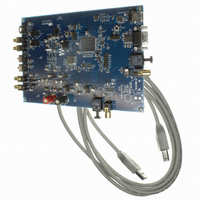
Manufacturer Part Number
CDB4265
Description
BOARD EVAL FOR CS4265 CODEC
Manufacturer
Cirrus Logic Inc
Specifications of CDB4265
Main Purpose
Audio, CODEC
Embedded
No
Utilized Ic / Part
CS4265
Primary Attributes
Stereo, 24-Bit, 192 kHz Sample Rate
Secondary Attributes
Graphic User Interface, S/PDIF/ I2S / I2C / SPI Interface
Description/function
Audio CODECs
Operating Supply Voltage
5 V
Product
Audio Modules
For Use With/related Products
CS4265
Lead Free Status / RoHS Status
Contains lead / RoHS non-compliant
Lead Free Status / RoHS Status
Lead free / RoHS Compliant, Contains lead / RoHS non-compliant
Other names
598-1001


DS657F2
4.11
4.12
4.12.1 TxOut Driver
Mute Control
The MUTEC pin becomes active during power-up initialization, reset, muting, if the MCLK to LRCK ratio is
incorrect, and during power-down. The MUTEC pin is intended to be used as control for an external mute
circuit in order to add off-chip mute capability.
Use of the Mute Control function is not mandatory but recommended for designs requiring the absolute min-
imum in extraneous clicks and pops. Also, use of the Mute Control function can enable the system designer
to achieve idle channel noise/signal-to-noise ratios which are only limited by the external mute circuit. The
MUTEC pin is an active-low CMOS driver. See
AES3 Transmitter
The CS4265 includes an IEC60958-3 digital audio transmitter. A comprehensive buffering scheme provides
write access to the channel status data. This buffering scheme is described in the
Management” section on page
The IEC60958-3 transmitter encodes and transmits audio and digital data according to the IEC60958-3
(S/PDIF) interface standard. The transmitter receives audio data from the input pin TXSDIN and control
clocks from the PCM Serial Interface. Audio and control data are multiplexed together and bi-phase mark
encoded. The resulting bit stream is driven from the output pin TXOUT to an output connector either directly
or through a transformer. The transmitter is clocked from the clock input pin MCLK.
The channel status (C) bits in the transmitted data stream are taken from storage areas within the CS4265.
The user can manually access the internal storage of the CS4265 to configure the transmitted channel sta-
tus data. The
the storage areas. The CS4265 transmits all ‘0’s in the user (U) data fields.
The line driver is a low skew, low impedance, single-ended output capable of driving cables directly. The
driver is set to ground during reset (RESET = LOW), when no transmit clock is provided, and optionally
CS4265
“Channel Status Buffer Management” section
MUTEC
AOUT
Figure 14. Suggested Active-Low Mute Circuit
LPF
52.
+V
-V
EE
EE
Figure 14
Couple
AC
MMUN2111LT1
+V
for a suggested active-low mute circuit.
A
describes the method of manually accessing
-V
47 kΩ
EE
10 kΩ
560 Ω
2 kΩ
“Channel Status Buffer
Audio
Out
CS4265
29
Related parts for CDB4265
Image
Part Number
Description
Manufacturer
Datasheet
Request
R

Part Number:
Description:
Development Kit
Manufacturer:
Cirrus Logic Inc
Datasheet:
Part Number:
Description:
Development Kit
Manufacturer:
Cirrus Logic Inc
Datasheet:


Part Number:
Description:
High-efficiency PFC + Fluorescent Lamp Driver Reference Design
Manufacturer:
Cirrus Logic Inc
Datasheet:
Part Number:
Description:
Development Kit
Manufacturer:
Cirrus Logic Inc
Datasheet:
Part Number:
Description:
Development Kit
Manufacturer:
Cirrus Logic Inc
Datasheet:

Part Number:
Description:
Development Kit
Manufacturer:
Cirrus Logic Inc
Datasheet:
Part Number:
Description:
Development Kit
Manufacturer:
Cirrus Logic Inc
Datasheet:
Part Number:
Description:
Development Kit
Manufacturer:
Cirrus Logic Inc
Datasheet:
Part Number:
Description:
Development Kit
Manufacturer:
Cirrus Logic Inc
Datasheet:

Part Number:
Description:
EVALUATION BOARD FOR CS8427
Manufacturer:
Cirrus Logic Inc
Datasheet:

Part Number:
Description:
BOARD EVAL FOR CS8416 RCVR
Manufacturer:
Cirrus Logic Inc
Datasheet:

Part Number:
Description:
EVALUATION BOARD FOR CS8420
Manufacturer:
Cirrus Logic Inc
Datasheet:

Part Number:
Description:
KIT DEVELOPMENT EP9315 ARM9
Manufacturer:
Cirrus Logic Inc
Datasheet:

Part Number:
Description:
KIT DEVELOPMENT EP9302 ARM9
Manufacturer:
Cirrus Logic Inc
Datasheet: