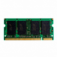
MT16VDDF12864HG-40BF2 Micron Technology Inc, MT16VDDF12864HG-40BF2 Datasheet - Page 19

MT16VDDF12864HG-40BF2
Manufacturer Part Number
MT16VDDF12864HG-40BF2
Description
MODULE DDR SDRAM 1GB 200-SODIMM
Manufacturer
Micron Technology Inc
Specifications of MT16VDDF12864HG-40BF2
Memory Type
DDR SDRAM
Memory Size
1GB
Speed
400MT/s
Package / Case
200-SODIMM
Main Category
DRAM Module
Sub-category
DDR SDRAM
Module Type
200SODIMM
Device Core Size
64b
Organization
128Mx64
Total Density
1GByte
Chip Density
512Mb
Maximum Clock Rate
400MHz
Operating Supply Voltage (typ)
2.6V
Operating Current
1.6A
Number Of Elements
16
Operating Supply Voltage (max)
2.7V
Operating Supply Voltage (min)
2.5V
Operating Temp Range
0C to 70C
Operating Temperature Classification
Commercial
Pin Count
200
Mounting
Socket
Lead Free Status / RoHS Status
Contains lead / RoHS non-compliant
pdf: 09005aef80b57837, source: 09005aef80b577fa
DDAF16C64_128x64HG.fm - Rev. D 9/04 EN
22. The valid data window is derived by achieving
23. Each byte lane has a corresponding DQS.
24. This limit is actually a nominal value and does not
25. To maintain a valid level, the transitioning edge of
26. JEDEC specifies CK and CK# input slew rate must
27. DQ and DM input slew rates must not deviate
28. V
29. The clock is allowed up to ±150ps of jitter. Each
30.
31. READs and WRITEs with auto precharge are not
32. Any positive glitch in the nominal voltage must be
the DRAM controller greater than eight refresh
cycles is not allowed.
other specifications:
(
directly porportional with the clock duty cycle
and a practical data valid window can be derived.
The clock is allowed a maximum duty cycle varia-
tion of 45/55, beyond which functionality is
uncertain.
result in a fail value. CKE is HIGH during
REFRESH command period (
CKE is LOW (i.e., during standby).
the input must:
be 1V/ns (2V/ns differentially).
from DQS by more than 10 percent. If the DQ/
DM/DQS slew rate is less than 0.5V/ns, timing
must be derated: 50ps must be added to
t
slew rate exceeds 4V/ns, functionality is uncer-
tain.
not active while any bank is active.
timing parameter is allowed to vary by the same
amount.
t
minimum actually applied to the device CK and
CK# inputs, collectively during bank active.
allowed to be issued until
fied prior to the internal precharge command
being issued.
less than 1/3 of the clock and must not exceed
+400mV or 2.9V, whichever is less. Any negative
glitch must be less than 1/3 of the clock cycle and
not exceed either -300mV or 2.2V, whichever is
more positive.
DH for each 100mv/ns reduction in slew rate. If
HP min is the lesser of
a. Sustain a constant slew rate from the current
b. Reach at least the target AC level.
c. After the AC target level is reached, continue to
t
QH =
DD
AC level through to the target AC level, V
or V
maintain at least the target DC level, V
or V
must not vary more than 4 percent if CKE is
t
IH
IH
HP -
(AC).
(DC).
t
QHS). The data valid window derates
t
HP (
t
t
t
CK/2),
CL minimum and
RAS (MIN) can be satis-
t
RFC [MIN]) else
t
DQSQ, and
t
DS and
IL
IL
(DC)
(AC)
t
t
QH
CH
19
33. Normal Output Drive Curves:
34. The voltage levels used are derived from a mini-
35. V
36. V
37.
38.
mum V
practice, the voltage levels obtained from a prop-
erly terminated bus will provide significantly dif-
ferent voltage values.
pulse width
greater than 1/3 of the cycle rate. V
V
pulse width can not be greater than 1/3 of the
cycle rate.
t
t
over
t
referenced to a specific voltage level but specify
when the device output is no longer driving
(
512MB, 1GB (x64, DR) PC3200
a. The full variation in driver pull-down current
b. The variation in driver pull-down current
c. The full variation in driver pull-up current
d. The variation in driver pull-up current within
e. The full variation in the ratio of the maximum
f. The full variation in the ratio of the nominal
HZ (MAX) will prevail over
RPST (MAX) condition.
RPST end point and
t
Micron Technology, Inc., reserves the right to change products or specifications without notice.
IH
IL
DD
RPST), or begins driving (
from minimum to maximum process, temper-
ature and voltage will lie within the outer
bounding lines of the V-I curve of Figure 8,
Pull-Down Characteristics, on page 20.
within nominal limits of voltage and tempera-
ture is expected, but not guaranteed, to lie
within the inner bounding lines of the V-I
curve of Figure 8, Pull-Down Characteristics,
on page 20.
from minimum to maximum process, temper-
ature and voltage will lie within the outer
bounding lines of the V-I curve of Figure 9,
Pull-Up Characteristics, on page 20.
nominal limits of voltage and temperature is
expected, but not guaranteed, to lie within the
inner bounding lines of the V-I curve of
Figure 9, Pull-Up Characteristics, on page 20.
to minimum pull-up and pull-down current
should be between 0.71 and 1.4, for device
drain-to-source voltages from 0.1V to 1.0V, and
at the same voltage and temperature.
pull-up to pull-down current should be unity
±10 percent, for device drain-to-source volt-
ages from 0.1V to 1.0V.
(MIN) = -1.5V for a pulse width
and V
t
overshoot: V
DQSCK (MIN) +
DD
DD
level and the referenced test load. In
200-PIN DDR SODIMM
Q must track each other.
3ns and the pulse width can not be
IH
(MAX) = V
t
RPRE (MAX) condition.
t
RPRE begin point are not
t
t
LZ (MIN) will prevail
RPRE).
t
DQSCK (MAX) +
DD
©2004 Micron Technology, Inc.
Q + 1.5V for a
IL
undershoot:
3ns and the


