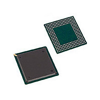
IDT72P51339L6BBI8 IDT, Integrated Device Technology Inc, IDT72P51339L6BBI8 Datasheet - Page 22

IDT72P51339L6BBI8
Manufacturer Part Number
IDT72P51339L6BBI8
Description
IC FLOW CTRL 36BIT 256-BGA
Manufacturer
IDT, Integrated Device Technology Inc
Datasheet
1.IDT72P51339L6BB8.pdf
(87 pages)
Specifications of IDT72P51339L6BBI8
Configuration
Dual
Density
576Kb
Access Time (max)
3.7ns
Word Size
36b
Organization
2Kx36x8
Sync/async
Synchronous
Expandable
Yes
Bus Direction
Uni-Directional
Package Type
BGA
Clock Freq (max)
166MHz
Supply Current
150mA
Operating Temp Range
-40C to 85C
Operating Temperature Classification
Industrial
Mounting
Surface Mount
Pin Count
256
Lead Free Status / RoHS Status
Contains lead / RoHS non-compliant
Other names
72P51339L6BBI8
Available stocks
Company
Part Number
Manufacturer
Quantity
Price
Company:
Part Number:
IDT72P51339L6BBI8
Manufacturer:
IDT, Integrated Device Technology Inc
Quantity:
10 000
TABLE 1 — DEVICE PROGRAMMING MODE COMPARISON
FUNCTIONAL DESCRIPTION
MASTER RESET
to HIGH. During a master reset all internal multi-queue device setup and control
registers are initialized and require programming either serially by the user via
the serial port, or via parallel programming or by using the default settings. Refer
to Figure 4, Device Programming Hierarchy for the programming hierarchy
structure. During a master reset the state of the following inputs determine the
functionality of the part, these pins should be held HIGH or LOW.
TABLE 2 — SETTING THE QUEUE PROGRAMMING MODE DURING MASTER RESET
IDT72P51339/72P51349/72P51359/72P51369 1.8V, MQ FLOW-CONTROL DEVICES
(8 QUEUES) 36 BIT WIDE CONFIGURATION 589, 824, 1,179,648, 2,359,296, and 4,718,592
Programmable Parameter Serial Programming
Number of Queues
Queue Depth
PAE / PAF Offset Value
Bus Matching
I/O voltage
A Master Reset is performed by toggling the MRS input from HIGH to LOW
PKT – Packet Mode
FM – Flag bus Mode
BM [3:0] – Bus Matching options
MAST – Master Device
ID0, 1, 2 – Device ID
Default mode
(DFM)
MRS
QSEL0
QSEL1
Any number from 1 to 8
Each queue depth can be
individualized
Programmable to any value
Any combination of x9 or x18 or x36 can Any combination of x9 or x18 or x36
be selected using the BM[3:0] bits.
LVTTL, eHSTL, HSTL
MRS
Default
(DFM)
Mode
See Table 2 for definition of value
See Table 2 for definition of value
DFM = LOW for Serial Programming mode
0
0
0
0
1
1
1
1
QSEL 1 QSEL 0
0
0
1
1
0
0
1
1
Figure 3. Reference Signals
0
1
0
1
0
1
0
1
Parallel Programming
Any number from 1 to 8
across the queues
Fixed value
LVTTL, eHSTL, HSTL
The total memory is evenly divided
can be selected using the BM[3:0] bits. be selected using the BM[3:0] bits
RESERVED
RESERVED
RESERVED
Serial programming mode
Enables the user to program the number
of Queues using the Write Address bus
Enables the user to program the number
of Queues using the Read Address bus
Selects 4 Queue
Selects 8 Queue
Queue Programming Method
22
serially or via the default method before any read/write operations can begin.
PROGRAMMING MODE CAPTURED
DEFAULT) are captured. Once the programming mode signals are captured
(latched), refer to Table 1 for details. It will then require a number of clock cycles
for the device to complete the configuration. Configuration completion is indicated
when the SENO signal transitions from high to low. The configuration completion
indication is consistent with the previous MQ device.
DFM – Programming mode, serial or default
DF – Offset value for PAE and PAF
Once a master reset has taken place, the device must be programmed either
See Figure 37, Master Reset for relevant timing.
On the rising of /MRS the programming mode signals (QSEL 0 &1,
6716 drw07
Any combination of x9, x18, or x36 can
Default Programming
4 or 8
The total memory is evenly divided
across the queues
Fixed value
LVTTL, eHSTL, HSTL
COMMERCIAL AND INDUSTRIAL
TEMPERATURE RANGES
6716 drw06
AUGUST 4, 2005


