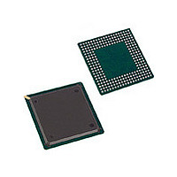
IDT72V7250L10BB IDT, Integrated Device Technology Inc, IDT72V7250L10BB Datasheet - Page 6

IDT72V7250L10BB
Manufacturer Part Number
IDT72V7250L10BB
Description
IC FIFO 4096X36 10NS 256BGA
Manufacturer
IDT, Integrated Device Technology Inc
Series
72Vr
Datasheet
1.IDT72V7230L15BB.pdf
(42 pages)
Specifications of IDT72V7250L10BB
Function
Asynchronous, Synchronous
Memory Size
147K (4K x 36)
Data Rate
100MHz
Access Time
10ns
Voltage - Supply
3.15 V ~ 3.45 V
Operating Temperature
0°C ~ 70°C
Mounting Type
Surface Mount
Package / Case
256-BGA
Configuration
Dual
Density
144Kb
Access Time (max)
6.5ns
Word Size
72b
Organization
2Kx72
Sync/async
Synchronous
Expandable
Yes
Bus Direction
Uni-Directional
Package Type
BGA
Clock Freq (max)
100MHz
Operating Supply Voltage (typ)
3.3V
Operating Supply Voltage (min)
3.15V
Operating Supply Voltage (max)
3.45V
Supply Current
75mA
Operating Temp Range
0C to 70C
Operating Temperature Classification
Commercial
Mounting
Surface Mount
Pin Count
256
Lead Free Status / RoHS Status
Contains lead / RoHS non-compliant
Other names
72V7250L10BB
Available stocks
Company
Part Number
Manufacturer
Quantity
Price
Company:
Part Number:
IDT72V7250L10BB
Manufacturer:
IDT, Integrated Device Technology Inc
Quantity:
10 000
PIN DESCRIPTION (CONTINUED)
NOTE:
1. These pins are for the JTAG port. Please refer to pages 22-25 and Figures 5-7.
IDT72V7230/7240/7250/7260/7270/7280/7290/72100 3.3V HIGH DENSITY SUPERSYNC II
512 x 72, 1K x 72, 2K x 72, 4K x 72, 8K x 36, 16K x 72, 32K x 72, 64K x 72
Symbol
EF/OR
PAF
PAE
HF
Q
TCK
TDI
TDO
TMS
TRST
0
–Q
(1)
(1)
(1)
(1)
71
(1)
Empty Flag/
Output Ready
Programmable
Almost-Full Flag
Programmable
Almost-Empty
Half-Full Flag
Data Outputs
JTAG Clock
JTAG Test Data Input
JTAG Test Data Output
JTAG Mode Select
JTAG Reset
Name
I/O
O
O
O
O
O
O
I
I
I
I
In the IDT Standard mode, the EF function is selected. EF indicates whether or not the FIFO memory is empty.
In FWFT mode, the OR function is selected. OR indicates whether or not there is valid data available at the outputs.
PAF goes HIGH if the number of free locations in the FIFO memory is more than offset m, which is stored in
PAE goes LOW if the number of words in the FIFO memory is less than offset n, which is stored in the Empty
offset n.
HF indicates whether the FIFO memory is more or less than half-full.
Data outputs for an 72-, 36- or 18-bit bus. When in 36- or 18-bit mode, the unused output pins should not
be connected. Data Outputs are not 5V tolerant regardless of the state of the OE and RCS.
Clock input for JTAG function. One of four terminals required by IEEE Standard 1149.1-1990. Test operations
of the device are synchronous to TCK. Data from TMS and TDI are sampled on the rising edge of TCK and
outputs change on the falling edge of TCK. If the JTAG function is not used this signal needs to be tied to GND.
One of four terminals required by IEEE Standard 1149.1-1990. During the JTAG boundary scan operation,
test data serially loaded via the TDI on the rising edge of TCK to either the Instruction Register, ID Register
and Bypass Register. An internal pull-up resistor forces TDI HIGH if left unconnected.
One of four terminals required by IEEE Standard 1149.1-1990. During the JTAG boundary scan operation,
test data serially loaded output via the TDO on the falling edge of TCK from either the Instruction Register, ID
Register and Bypass Register. This output is high impedance except when shifting, while in SHIFT-DR and
SHIFT-IR controller states.
TMS is a serial input pin. One of four terminals required by IEEE Standard 1149.1-1990. TMS directs the
the device through its TAP controller states. An internal pull-up resistor forces TMS HIGH if left unconnected.
TRST is an asynchronous reset pin for the JTAG controller. The JTAG TAP controller does not automatically
reset upon power-up, thus it must be reset by either this signal or by setting TMS= HIGH for five TCK cycles.
If the TAP controller is not properly reset then the FIFO outputs will always be in high-impedance. If the JTAG
function is used but the user does not want to use TRST, then TRST can be tied with MRS to ensure proper
FIFO operation. If the JTAG function is not used then this signal needs to be tied to GND.
the Full Offset register. PAF goes LOW if the number of free locations in the FIFO memory is less than or
equal to m.
Offset register. PAE goes HIGH if the number of Flag words in the FIFO memory is greater than or equal to
6
Description
TM
FIFO
COMMERCIAL TEMPERATURE RANGE


