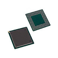
IDT72V7250L10BB IDT, Integrated Device Technology Inc, IDT72V7250L10BB Datasheet - Page 23

IDT72V7250L10BB
Manufacturer Part Number
IDT72V7250L10BB
Description
IC FIFO 4096X36 10NS 256BGA
Manufacturer
IDT, Integrated Device Technology Inc
Series
72Vr
Datasheet
1.IDT72V7230L15BB.pdf
(42 pages)
Specifications of IDT72V7250L10BB
Function
Asynchronous, Synchronous
Memory Size
147K (4K x 36)
Data Rate
100MHz
Access Time
10ns
Voltage - Supply
3.15 V ~ 3.45 V
Operating Temperature
0°C ~ 70°C
Mounting Type
Surface Mount
Package / Case
256-BGA
Configuration
Dual
Density
144Kb
Access Time (max)
6.5ns
Word Size
72b
Organization
2Kx72
Sync/async
Synchronous
Expandable
Yes
Bus Direction
Uni-Directional
Package Type
BGA
Clock Freq (max)
100MHz
Operating Supply Voltage (typ)
3.3V
Operating Supply Voltage (min)
3.15V
Operating Supply Voltage (max)
3.45V
Supply Current
75mA
Operating Temp Range
0C to 70C
Operating Temperature Classification
Commercial
Mounting
Surface Mount
Pin Count
256
Lead Free Status / RoHS Status
Contains lead / RoHS non-compliant
Other names
72V7250L10BB
Available stocks
Company
Part Number
Manufacturer
Quantity
Price
Company:
Part Number:
IDT72V7250L10BB
Manufacturer:
IDT, Integrated Device Technology Inc
Quantity:
10 000
JTAG INTERFACE
support the JTAG boundary scan interface. The IDT72V7230/72V7240/
72V7250/72V7260/72V7270/72V7280/72V7290/72V72100 incorporates
the necessary tap controller and modified pad cells to implement the JTAG facility.
program files for these devices.
TEST ACCESS PORT (TAP)
internal of the processor. It consists of four input ports (TCLK, TMS, TDI, TRST)
and one output port (TDO).
IDT72V7230/7240/7250/7260/7270/7280/7290/72100 3.3V HIGH DENSITY SUPERSYNC II
512 x 72, 1K x 72, 2K x 72, 4K x 72, 8K x 36, 16K x 72, 32K x 72, 64K x 72
Five additional pins (TDI, TDO, TMS, TCK and TRST) are provided to
Note that IDT provides appropriate Boundary Scan Description Language
The Tap interface is a general-purpose port that provides access to the
TDO
TDI
TMS
TCLK
TRST
T
A
P
Cont-
roller
TAP
clkDR, ShiftDR
clklR, ShiftlR
UpdatelR
UpdateDR
Figure 6. Boundary Scan Architecture
Instruction Register
23
Control Signals
complete description refer to the IEEE Standard Test Access Port Specification
(IEEE Std. 1149.1-1990).
THE TAP CONTROLLER
TMS and TCLK signals to generate clock and control signals to the Instruction
and Data Registers for capture and update of data.
DeviceID Reg.
Boundary Scan Reg.
Bypass Reg.
The Standard JTAG interface consists of four basic elements:
• • • • •
• • • • •
• • • • •
• • • • •
The following sections provide a brief description of each element. For a
The Figure below shows the standard Boundary-Scan Architecture
The Tap controller is a synchronous finite state machine that responds to
Test Access Port (TAP)
TAP controller
Instruction Register (IR)
Data Register Port (DR)
Instruction Decode
TM
FIFO
COMMERCIAL TEMPERATURE RANGE
Mux
4680 drw11


