IDT72V7250L10BB IDT, Integrated Device Technology Inc, IDT72V7250L10BB Datasheet - Page 13
IDT72V7250L10BB
Manufacturer Part Number
IDT72V7250L10BB
Description
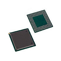
IC FIFO 4096X36 10NS 256BGA
Manufacturer
IDT, Integrated Device Technology Inc
Series
72Vr
Datasheet
1.IDT72V7230L15BB.pdf
(42 pages)
Specifications of IDT72V7250L10BB
Function
Asynchronous, Synchronous
Memory Size
147K (4K x 36)
Data Rate
100MHz
Access Time
10ns
Voltage - Supply
3.15 V ~ 3.45 V
Operating Temperature
0°C ~ 70°C
Mounting Type
Surface Mount
Package / Case
256-BGA
Configuration
Dual
Density
144Kb
Access Time (max)
6.5ns
Word Size
72b
Organization
2Kx72
Sync/async
Synchronous
Expandable
Yes
Bus Direction
Uni-Directional
Package Type
BGA
Clock Freq (max)
100MHz
Operating Supply Voltage (typ)
3.3V
Operating Supply Voltage (min)
3.15V
Operating Supply Voltage (max)
3.45V
Supply Current
75mA
Operating Temp Range
0C to 70C
Operating Temperature Classification
Commercial
Mounting
Surface Mount
Pin Count
256
Lead Free Status / RoHS Status
Contains lead / RoHS non-compliant
Other names
72V7250L10BB
Available stocks
Company
Part Number
Manufacturer
Quantity
Price
Company:

Part Number:
IDT72V7250L10BB
Manufacturer:
IDT, Integrated Device Technology Inc
Quantity:
10 000


IDT72V7230/7240/7250/7260/7270/7280/7290/72100 3.3V HIGH DENSITY SUPERSYNC II
512 x 72, 1K x 72, 2K x 72, 4K x 72, 8K x 36, 16K x 72, 32K x 72, 64K x 72
D/Q35
D/Q35
D/Q17
D/Q17
D/Q71
D/Q71
1st Parallel Offset Write/Read Cycle
2nd Parallel Offset Write/Read Cycle
D/Q16
D/Q16
16
16
16
15
15
16
15
14
15
14
D/Q19
D/Q19
D/Q19
D/Q19
EMPTY OFFSET (LSB) REGISTER (PAE)
FULL OFFSET (LSB) REGISTER (PAF)
14
13
14
13
D/Q17
D/Q17
13
12
13
12
D/Q17
D/Q17
1st Parallel Offset Write/Read Cycle
2nd Parallel Offset Write/Read Cycle
1st Parallel Offset Write/Read Cycle
2nd Parallel Offset Write/Read Cycle
Data Inputs/Outputs
Data Inputs/Outputs
12
11
12
11
16
16
16
16
EMPTY OFFSET REGISTER (PAE)
EMPTY OFFSET REGISTER (PAE)
11
11
10
10
16
15
FULL OFFSET REGISTER (PAF)
16
15
16
15
FULL OFFSET REGISTER (PAF)
15
Figure 3. Programmable Flag Offset Programming Sequence (Continued)
16
10
10
9
14
15
14
15
14
15
14
9
15
x18 Bus Width
D/Q8
D/Q8
14
13
14
13
9
14
13
14
13
9
13
8
8
13
12
12
13
12
13
12
8
8
11
12
7
7
11
12
12
12
11
11
7
7
x36 Bus Width
x72 Bus Width
6
6
11
11
10
11
10
11
6
10
10
6
# of Bits Used
5
5
10
10
10
10
5
5
9
9
9
9
D/Q8
D/Q8
D/Q8
D/Q8
4
4
9
4
4
9
9
9
3
3
3
3
8
8
8
8
8
8
8
8
2
2
2
2
7
7
7
7
7
7
7
7
# of Bits Used
# of Bits Used
# of Bits Used
# of Bits Used
D/Q0
D/Q0
13
1
1
1
1
6
6
6
6
6
6
6
6
5
5
5
5
5
5
5
5
Non-Interspersed
Parity
Interspersed
Parity
4
4
4
4
4
4
4
4
3
3
3
3
3
3
3
3
TM
2
2
2
2
2
2
2
2
FIFO
D/Q0
D/Q0
D/Q0
D/Q0
1
1
1
1
1
1
1
1
Non-Interspersed
Parity
Non-Interspersed
Parity
Non-Interspersed
Parity
Interspersed
Parity
Non-Interspersed
Parity
Interspersed
Parity
Interspersed
Parity
Interspersed
Parity
COMMERCIAL TEMPERATURE RANGE
# of Bits Used:
09 bits for the IDT72V7230
10 bits for the IDT72V7240
11 bits for the IDT72V7250
12 bits for the IDT72V7260
13 bits for the IDT72V7270
14 bits for the IDT72V7280
15 bits for the IDT72V7290
16 bits for the IDT72V72100
Note: All unused input bits
are don’t care.
4680 drw07
Related parts for IDT72V7250L10BB
Image
Part Number
Description
Manufacturer
Datasheet
Request
R

Part Number:
Description:
TRANSLATION DEVICE DPI 80-PQFP
Manufacturer:
IDT, Integrated Device Technology Inc
Datasheet:
Part Number:
Description:
IDT PART
Manufacturer:
IDT, Integrated Device Technology Inc
Datasheet:
Part Number:
Description:
IC LIU T1/E1/J1 OCTAL 256PBGA
Manufacturer:
IDT, Integrated Device Technology Inc
Datasheet:

Part Number:
Description:
IC FREQ TIMING GENERATOR 28TSSOP
Manufacturer:
IDT, Integrated Device Technology Inc
Datasheet:
Part Number:
Description:
IC CLK DVR PLL 1:10 40VFQFPN
Manufacturer:
IDT, Integrated Device Technology Inc
Datasheet:
Part Number:
Description:
IC CLK FANOUT BUFFER 1:18 32LQFP
Manufacturer:
IDT, Integrated Device Technology Inc
Datasheet:
Part Number:
Description:
IC CLK FANOUT BUFFER 1:18 32LQFP
Manufacturer:
IDT, Integrated Device Technology Inc
Datasheet:
Part Number:
Description:
IC CK505 VREG/RES 56TSSOP
Manufacturer:
IDT, Integrated Device Technology Inc
Datasheet:

Part Number:
Description:
IC SDRAM CLK DVR 1:10 48-TSSOP
Manufacturer:
IDT, Integrated Device Technology Inc
Datasheet:

Part Number:
Description:
IC CLK DVR PLL 1:10 48TSSOP
Manufacturer:
IDT, Integrated Device Technology Inc
Datasheet:
Part Number:
Description:
IC FLEXPC CLK PROGR P4 56-TSSOP
Manufacturer:
IDT, Integrated Device Technology Inc
Datasheet:
Part Number:
Description:
IC FLEXPC CLK PROGR P4 56-TSSOP
Manufacturer:
IDT, Integrated Device Technology Inc
Datasheet:
Part Number:
Description:
IC FLEXPC CLK PROGR P4 56-SSOP
Manufacturer:
IDT, Integrated Device Technology Inc
Datasheet:

Part Number:
Description:
IC PLL CLK DRIVER 2.5V 28-TSSOP
Manufacturer:
IDT, Integrated Device Technology Inc
Datasheet:
Part Number:
Description:
IC CLOCK DRIVER 2.5V 24-TSSOP
Manufacturer:
IDT, Integrated Device Technology Inc
Datasheet: