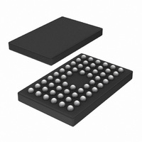
PTN3700EV/G,118 NXP Semiconductors, PTN3700EV/G,118 Datasheet - Page 9

PTN3700EV/G,118
Manufacturer Part Number
PTN3700EV/G,118
Description
IC MOBILE INTERFACE 56-VFBGA
Manufacturer
NXP Semiconductors
Type
Interfacer
Series
-r
Datasheet
1.PTN3700EVG118.pdf
(41 pages)
Specifications of PTN3700EV/G,118
Package / Case
56-VFBGA
Applications
Mobile Phones, Cellular, Video Displays
Mounting Type
Surface Mount
Input Current
4 uA
Maximum Operating Temperature
+ 85 C
Minimum Operating Temperature
- 40 C
Mounting Style
SMD/SMT
Operating Supply Voltage
1.8 V
Supply Voltage (max)
1.95 V
Supply Voltage (min)
1.65 V
Number Of Outputs
4
Lead Free Status / RoHS Status
Lead free / RoHS Compliant
Lead Free Status / RoHS Status
Lead free / RoHS Compliant, Lead free / RoHS Compliant
Other names
935284074118
PTN3700EV/G-T
PTN3700EV/G-T
PTN3700EV/G-T
PTN3700EV/G-T
Available stocks
Company
Part Number
Manufacturer
Quantity
Price
Company:
Part Number:
PTN3700EV/G,118
Manufacturer:
NXP Semiconductors
Quantity:
10 000
NXP Semiconductors
7. Functional description
PTN3700_1
Product data sheet
7.1 General
A complete simple mobile interface link consists of one PTN3700 configured as
transmitter (see
channels; and one PTN3700 configured as receiver (see
ground are supplied to pins VDD and GND respectively (power and ground should be
routed and decoupled to analog supply pin VDDA and ground pin GNDA separately for
lowest jitter operation). Configuration of either transmitter or receiver mode is achieved by
strapping the CMOS input pin TX/RX HIGH or LOW, respectively.
Configured as transmitter, PTN3700 accepts parallel CMOS input data including color
pixel data (R[7:0], G[7:0], B[7:0]), three control bits HS (horizontal synchronization), VS
(vertical synchronization), DE (data enable), auxiliary bits A[1:0] and pixel clock PCLK.
The PTN3700 calculates a parity bit (excluding the auxiliary bits, see
serializes the data and outputs as a high-speed serial data stream on up to three
subLVDS differential outputs (D0+, D0 , D1+, D1 , D2+, D2 ) depending on the
serialization mode selected by pins LS[1:0] (see
generates internally the bit clock used for serialization of video input data, parity bit and
control bits, and outputs along with the serial output data a differential pixel clock on
differential subLVDS output pair CLK+ and CLK .
Configured as receiver, PTN3700 accepts serial differential data inputs D0+, D0 , D1+,
D1 , D2+, D2 and differential input clock CLK+ and CLK from the signaling channel and
deserializes the received data into parallel output data on pins R[7:0], G[7:0], B[7:0], HS,
VS, DE and A[1:0] along with the PLL-regenerated pixel clock PCLK. Also, a parity
checking function is performed on the incoming R[7:0], G[7:0], B[7:0], HS, VS, DE bits and
an error flagged by signaling a HIGH state on CMOS output pin CPO (see
Serialization mode pins LS[1:0] need to be selected according to the expected
serialization mode (see
subLVDS differential serial inputs. To minimize EMI, the parallel outputs can be configured
by tying pin F/XS either HIGH or LOW to output fast or slow output slew rates respectively.
The PTN3700 is capable of operating in either of two distinct transmission modes: Pseudo
Source Synchronous mode (PSS), and Full (or ‘true’) Source Synchronous mode (FSS),
selected by CMOS input pin FSS. In PSS mode, the pixel clock PCLK is used both as the
transmission frequency reference and its rising edge as the delineation of the start of a
pixel. This transmission mode relies on the Receiver PLL to reconstruct the bit clock at the
receiving end. In FSS mode, the bit clock is transmitted (in DDR mode) instead of the pixel
clock. Rather than achieve frame boundary detection using the pixel clock edge as in PSS
mode, in FSS mode the Transmitter encodes ‘synchronization words’ over the link which
are detected and used for data to pixel alignment by the Receiver. This methodology
guarantees false-synchronization-free transmission with zero protocol overhead.
The PTN3700 can be put into very low ‘Shutdown’ power state by tying CMOS input pin
XSD LOW. Additionally, the PTN3700 will automatically enter a low-power ‘Standby’ mode
when no active input clock is detected on its inputs (see
Figure
Rev. 01 — 14 August 2007
1); two, three or four differential-pair high-speed signaling
Section
7.2) to correctly receive and decode the up to three
1.8 V simple mobile interface link bridge IC
Section
Section
7.2). An integrated low-jitter PLL
Figure
2). Link power and
7.5).
Section
PTN3700
© NXP B.V. 2007. All rights reserved.
Section
7.6) and
7.6).
9 of 41


