PTN3700EV/G,118 NXP Semiconductors, PTN3700EV/G,118 Datasheet - Page 10
PTN3700EV/G,118
Manufacturer Part Number
PTN3700EV/G,118
Description
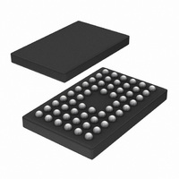
IC MOBILE INTERFACE 56-VFBGA
Manufacturer
NXP Semiconductors
Type
Interfacer
Series
-r
Datasheet
1.PTN3700EVG118.pdf
(41 pages)
Specifications of PTN3700EV/G,118
Package / Case
56-VFBGA
Applications
Mobile Phones, Cellular, Video Displays
Mounting Type
Surface Mount
Input Current
4 uA
Maximum Operating Temperature
+ 85 C
Minimum Operating Temperature
- 40 C
Mounting Style
SMD/SMT
Operating Supply Voltage
1.8 V
Supply Voltage (max)
1.95 V
Supply Voltage (min)
1.65 V
Number Of Outputs
4
Lead Free Status / RoHS Status
Lead free / RoHS Compliant
Lead Free Status / RoHS Status
Lead free / RoHS Compliant, Lead free / RoHS Compliant
Other names
935284074118
PTN3700EV/G-T
PTN3700EV/G-T
PTN3700EV/G-T
PTN3700EV/G-T
Available stocks
Company
Part Number
Manufacturer
Quantity
Price
Company:

Part Number:
PTN3700EV/G,118
Manufacturer:
NXP Semiconductors
Quantity:
10 000


NXP Semiconductors
Table 5.
[1]
PTN3700_1
Product data sheet
LS1
H
H
L
L
Mode 11 is used for test purposes only.
LS0
H
H
L
L
Link programmability
Mode
00
01
10
11
7.2 Link programmability
7.3 Versatile signal mirroring programmability
The number of high-speed serial channels used is programmed by CMOS input pins
LS[1:0]. For a given link consisting of a transmitter and receiver pair of PTN3700’s, the
number of channels used must be programmed identically or the link will malfunction. The
PTN3700, once programmed, will assume the corresponding serialization ratio as shown
in
used for production testing purposes only and should not be used in application.
The 1-lane mode is typically meant for smaller video display formats (e.g., QVGA to
HVGA), while the 2-lane mode is typically used for display formats like HVGA and VGA.
The 3-lane mode supports larger display formats such as VGA or XGA. Please see
Section 12.1
In order to provide flexibility for different signal order and flow requirements in different
applications, the PTN3700 can be programmed to mirror its signal order for the parallel
and serial I/Os independently using the PSEL[1:0] inputs. The signal order also changes
as a function of the TX/RX input by mirroring signals in such a way that the Transmitter
and Receiver in a given link can be connected without signal crossings by simply
opposing the two instances of PTN3700 and rotating one of them by 180 degrees. The
truth table for the versatile signal mirroring scheme is shown in
individual ball mappings are given in
Table
serial channels
high-speed
Number of
reserved
5. When pins LS[1:0] are both HIGH, the PTN3700 is put in a test mode which is
1
2
3
for more information.
[1]
frequency range (MHz)
Rev. 01 — 14 August 2007
Supported PCLK
20.0 to 65.0
4.0 to 21.6
8.0 to 43.3
reserved
Figure 4
1.8 V simple mobile interface link bridge IC
through
Guaranteed data
channel (Mbit/s)
bandwidth per
120 to 650
120 to 650
200 to 650
reserved
Figure
11.
Table 6
bandwidth (Mbit/s)
PTN3700
© NXP B.V. 2007. All rights reserved.
and
aggregate link
Guaranteed
reserved
Table
1300
1950
650
7. The
10 of 41
Related parts for PTN3700EV/G,118
Image
Part Number
Description
Manufacturer
Datasheet
Request
R

Part Number:
Description:
Serializers & Deserializers - Serdes 1.8V MOBILE INTERF LINK BRIDGE
Manufacturer:
NXP Semiconductors

Part Number:
Description:
1.8 V simple mobile interface link bridge IC Very low power profile
Manufacturer:
NXP [NXP Semiconductors]
Datasheet:
Part Number:
Description:
NXP Semiconductors designed the LPC2420/2460 microcontroller around a 16-bit/32-bitARM7TDMI-S CPU core with real-time debug interfaces that include both JTAG andembedded trace
Manufacturer:
NXP Semiconductors
Datasheet:

Part Number:
Description:
NXP Semiconductors designed the LPC2458 microcontroller around a 16-bit/32-bitARM7TDMI-S CPU core with real-time debug interfaces that include both JTAG andembedded trace
Manufacturer:
NXP Semiconductors
Datasheet:
Part Number:
Description:
NXP Semiconductors designed the LPC2468 microcontroller around a 16-bit/32-bitARM7TDMI-S CPU core with real-time debug interfaces that include both JTAG andembedded trace
Manufacturer:
NXP Semiconductors
Datasheet:
Part Number:
Description:
NXP Semiconductors designed the LPC2470 microcontroller, powered by theARM7TDMI-S core, to be a highly integrated microcontroller for a wide range ofapplications that require advanced communications and high quality graphic displays
Manufacturer:
NXP Semiconductors
Datasheet:
Part Number:
Description:
NXP Semiconductors designed the LPC2478 microcontroller, powered by theARM7TDMI-S core, to be a highly integrated microcontroller for a wide range ofapplications that require advanced communications and high quality graphic displays
Manufacturer:
NXP Semiconductors
Datasheet:
Part Number:
Description:
The Philips Semiconductors XA (eXtended Architecture) family of 16-bit single-chip microcontrollers is powerful enough to easily handle the requirements of high performance embedded applications, yet inexpensive enough to compete in the market for hi
Manufacturer:
NXP Semiconductors
Datasheet:
Part Number:
Description:
The XA-S3 device is a member of Philips Semiconductors? XA(eXtended Architecture) family of high performance 16-bitsingle-chip microcontrollers
Manufacturer:
NXP Semiconductors
Datasheet:

Part Number:
Description:
The NXP BlueStreak LH75401/LH75411 family consists of two low-cost 16/32-bit System-on-Chip (SoC) devices
Manufacturer:
NXP Semiconductors
Datasheet:
Part Number:
Description:
The NXP LPC3130/3131 combine an 180 MHz ARM926EJ-S CPU core, high-speed USB2
Manufacturer:
NXP Semiconductors
Datasheet:
Part Number:
Description:
The NXP LPC3141 combine a 270 MHz ARM926EJ-S CPU core, High-speed USB 2
Manufacturer:
NXP Semiconductors
Part Number:
Description:
The NXP LPC3143 combine a 270 MHz ARM926EJ-S CPU core, High-speed USB 2
Manufacturer:
NXP Semiconductors

Part Number:
Description:
The NXP LPC3152 combines an 180 MHz ARM926EJ-S CPU core, High-speed USB 2
Manufacturer:
NXP Semiconductors