PTN3700EV/G,118 NXP Semiconductors, PTN3700EV/G,118 Datasheet
PTN3700EV/G,118
Specifications of PTN3700EV/G,118
PTN3700EV/G-T
PTN3700EV/G-T
Available stocks


Related parts for PTN3700EV/G,118


PTN3700EV/G,118 Summary of contents
Page 1
PTN3700 1.8 V simple mobile interface link bridge IC Rev. 01 — 14 August 2007 1. General description The PTN3700 is a 1.8 V simple mobile interface link bridge IC which can function both as a transmitter-serializer or a receiver-deserializer ...
Page 2
... NXP Semiconductors The PTN3700 automatically rotates the order of the essential signals (parallel CMOS and high-speed serial data and clock) depending on whether it is operating as transmitter or as receiver (using pin TX/RX). In addition, two Pinning Select bits (inputs PSEL[1:0]) allow for four additional signal order configurations. This allows for various topologies of printed circuit board or fl ...
Page 3
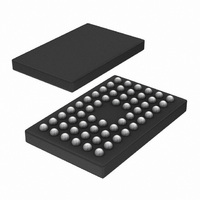
... NXP Semiconductors 4. Ordering information Table 1. Ordering information Type number Solder process PTN3700EV/G Pb-free (SnAgCu solder ball compound) [1] 0.5 mm ball pitch; 1.0 mm maximum package height. 4.1 Ordering options Table 2. Type number PTN3700EV/G 5. Functional diagram LS[1:0] PSEL[1:0] Fig 1. Functional diagram of PTN3700 in Transmitter mode ...
Page 4
... NXP Semiconductors D0+ D0 D1+ D1 D2+ D2 CLK+ CLK FM FSS F/XS XSD LS[1:0] PSEL[1:0] Fig 2. Functional diagram of PTN3700 in Receiver mode PTN3700_1 Product data sheet PTN3700 DESERIALIZER N PCLK PLL DDR SDR 2 2 TX/RX = LOW Rev. 01 — 14 August 2007 PTN3700 1.8 V simple mobile interface link bridge IC ...
Page 5
... NXP Semiconductors 6. Pinning information 6.1 Pinning Fig 3. Ball configuration for VFBGA56 D2+ VDDA GNDA VS PCLK C D1+ TX/RX A1 GND D D1 VDD PSEL0 LS0 E CLK+ GND PSEL1 LS1 F CLK F/XS A0 GND G D0+ XSD CPO R7 R5 56-ball grid; transparent top view Fig 4. VFBGA56 ball mapping - Transmitter mode (TX/RX = HIGH) ...
Page 6
... NXP Semiconductors D2+ VDDA GNDA D1+ TX/RX A1 GND D D1 VDD PSEL0 LS0 E CLK+ GND PSEL1 LS1 F CLK F/XS A0 GND G D0+ XSD VS PCLK H D0 CPO DE HS 56-ball grid; transparent top view Fig 8. VFBGA56 ball mapping - Receiver mode (TX/RX = LOW); PSEL[1:0] = 00b VDDA D0+ GNDA R6 R4 ...
Page 7
... NXP Semiconductors 6.2 Pin description Table 3. Pin description - Transmitter mode [1] Symbol Pin Type Parallel data inputs R[7:0], G[7:0], B[7:0] CMOS HS CMOS VS CMOS DE CMOS A0, A1 CMOS High-speed serial outputs D0 D1 SubLVDS D2+, D2 driver CLK+, CLK SubLVDS driver Clock inputs PCLK CMOS Configuration inputs ...
Page 8
... NXP Semiconductors Table 4. Pin description - Receiver mode [1] Symbol Pin Type Parallel data outputs R[7:0], G[7:0], B[7:0] CMOS HS CMOS VS CMOS DE CMOS A0, A1 CMOS High-speed serial inputs D0 D1+, SubLVDS D1 , D2+, D2 receiver CLK+, CLK SubLVDS receiver Clock outputs PCLK CMOS Configuration inputs TX/RX ...
Page 9
... NXP Semiconductors 7. Functional description 7.1 General A complete simple mobile interface link consists of one PTN3700 configured as transmitter (see channels; and one PTN3700 configured as receiver (see ground are supplied to pins VDD and GND respectively (power and ground should be routed and decoupled to analog supply pin VDDA and ground pin GNDA separately for lowest jitter operation). Confi ...
Page 10
... NXP Semiconductors 7.2 Link programmability The number of high-speed serial channels used is programmed by CMOS input pins LS[1:0]. For a given link consisting of a transmitter and receiver pair of PTN3700’s, the number of channels used must be programmed identically or the link will malfunction. The PTN3700, once programmed, will assume the corresponding serialization ratio as shown ...
Page 11
... NXP Semiconductors Table 6. Ball location [1] For PTN3700EV/G VFBGA56 package option. See also PTN3700_1 Product data sheet Versatile signal mirroring programmability - Parallel I/O [ (Receive mode PCLK Rev. 01 — 14 August 2007 PTN3700 1.8 V simple mobile interface link bridge IC TX/RX H PSEL0 H L (Transmit mode) ...
Page 12
... NXP Semiconductors Table 7. Ball location [1] For PTN3700EV/G VFBGA56 package option. See also 7.4 High-speed data channel protocol options The PTN3700 maps the transmission protocol in accordance with the serialization mode selected by pins LS[1:0]. In Mode 00 (1-channel), all RGB, parity and synchronization bits are serialized onto a single 30-bit sequence. In Mode 01 (2-channel), these bits are mapped onto two simultaneous 15-bit sequences divided across two lanes ...
Page 13
... NXP Semiconductors 7.4.1 Serial protocol bit mapping - pseudo source synchronous mode (FSS = LOW (differential) CLK (differential) Fig 12. Mode 00 - single serial data channel mode (FSS = LOW (differential (differential) CLK (differential) Fig 13. Mode 01 - dual serial data channel mode (FSS = LOW) D0 (differential) D1 (differential) D2 (differential) ...
Page 14
... NXP Semiconductors 7.4.2 Serial protocol bit mapping - fully source synchronous mode (FSS = HIGH (differential) CLK (differential) Fig 15. Mode 00 - single serial data channel mode (FSS = HIGH) (differential) (differential) CLK (differential) Fig 16. Mode 01 - dual serial data channel mode (FSS = HIGH) Fig 17. Mode 10 - triple serial data channel mode (FSS = HIGH) ...
Page 15
... NXP Semiconductors 7.4.3 PLL, PCLK, CLK and pixel synchronization 7.4.3.1 Pixel synchronization PSS mode: synchronization. At the receiver side, a PLL is needed to re-generate the bit clock, translating to a higher receiver power dissipation. FSS mode: synchronization words are transmitted in the non-active display area for pixel synchronization ...
Page 16
... NXP Semiconductors Table 8. FSS LOW HIGH [1] ‘X’ signifies that PTN3700 handles this signal transparently, i.e., data is transmitted and received as-is. [2] ‘R, G, B’ signifies that video data have to be input according to the exact chosen pin configuration of PTN3700, specifically: a) Bit order reversal is not allowed, even if both the transmit data and receive data are reversed in bit order. For example, the MSB of ‘ ...
Page 17
... NXP Semiconductors Fig 18. Typical video screen 7.5 Power modes The PTN3700 has three different power modes to minimize power consumption of the link as a function of link activity: Shutdown mode, Standby mode, and Active mode. The truth table for the three power modes is shown in • ...
Page 18
... NXP Semiconductors Table 10. Inputs XSD CLK+, CLK floating H stopped H running 7.6 Link error detection and correction In Transmitter mode, PTN3700 calculates an odd parity bit and merges this into the serialized output data stream to allow the receiver to detect whether parity has been violated for its received input data. The parity bit CP is calculated across the 27-bit input ...
Page 19
... NXP Semiconductors Table 12. Parity decoding function table - Receiver mode Inputs XSD Clock (R[7:0], G[7:0], B[7:0], HS, VS, DE) H running H running H running H running H stopped floating [1] YYY = current valid pixel data is output to the parallel interface. n [2] YYY = most recent valid pixel data is output to the parallel interface. ...
Page 20
... NXP Semiconductors 7.8 Auxiliary signals The two auxiliary bits A[1:0] are user-supplied bits that can be additionally serialized and deserialized by the PTN3700 in transmitter and receiver modes, respectively. These auxiliary bits are transparent to the PTN3700 and can be used to transmit and receive miscellaneous status or mode information across the link to the display. Note that the auxiliary bits A[1:0] are excluded from the parity calculation and detection in the transmitter and receiver modes respectively ...
Page 21
... NXP Semiconductors 10. Static characteristics Table 16. Static characteristics +85 C, unless otherwise specified. amb Symbol Parameter V supply voltage DD V HIGH-level input voltage IH V LOW-level input voltage IL V HIGH-level output voltage OH V LOW-level output voltage OL C input capacitance i Transmitter mode, PSS mode (TX/RX = HIGH; FSS = LOW) ...
Page 22
... NXP Semiconductors Table 16. Static characteristics +85 C, unless otherwise specified. amb Symbol Parameter Receiver mode, PSS mode (TX/RX = LOW; FSS = LOW) I supply current DD Receiver mode, FSS mode (TX/RX = LOW; FSS = HIGH) I supply current DD [1] Worst-case data pattern for power dissipation is used: alternating vertical stripes. The colors of the stripes correspond to the data pattern: RGB[23:0] = 0xAA AAAA (odd stripes) / RGB[23:0] = 0x55 5555 (even stripes) ...
Page 23
... NXP Semiconductors 11. Dynamic characteristics 11.1 Transmitter mode Table 17. Dynamic characteristics for Transmitter mode +85 C, unless otherwise specified. DD amb All CMOS input signals’ rise time and fall time to Transmitter are stipulated to be from ns. Symbol Parameter f input frequency on pin i(PCLK) ...
Page 24
... NXP Semiconductors 11.2 Receiver mode Table 18. Dynamic characteristics for Receiver mode +85 C, unless otherwise specified. DD amb CMOS output load pF. L Symbol Parameter f output frequency on o(PCLK) pin PCLK output duty cycle on o(PCLK) pin PCLK t data output skew time Mode 00; F/ ...
Page 25
... NXP Semiconductors Fig 20. AC timing diagram - Receiver mode PTN3700_1 Product data sheet 1.8 V simple mobile interface link bridge IC VS, HS, DE, R[7:0], G[7:0], B[7:0] t sk(Q) PCLK Rev. 01 — 14 August 2007 PTN3700 0. jit(r)PCLK 0.8V DD 0.2V DD 002aab368 © NXP B.V. 2007. All rights reserved. ...
Page 26
... NXP Semiconductors 11.3 Power-on/power-off sequence 11.3.1 Power-on sequence Table 19. Power-on sequence timing characteristics +85 C, unless otherwise specified. DD amb These values are for transitions of the Shutdown mode to the Standby mode and the Standby mode to the Active mode. Symbol Parameter t set-up time from V ...
Page 27
... NXP Semiconductors 11.3.2 Power-off sequence Table 20. Power-off sequence timing characteristics +85 C, unless otherwise specified. DD amb These values are for transition of the Active mode to the Standby mode. Symbol Parameter t delay time from PCLK LOW to transmitter d(PCLKL-TXQZ) data output float t receiver data input float to receiver ...
Page 28
... NXP Semiconductors 11.4 High-speed signaling channel Table 21. High-speed signaling channel SubLVDS output characteristics, Transmitter mode +85 C, unless otherwise specified. See DD amb Symbol Parameter V differential output O(dif) voltage V common-mode output O(cm) voltage V peak-to-peak ripple O(cm)ripple(p-p) common-mode output voltage R differential output ...
Page 29
... NXP Semiconductors Table 22. High-speed signaling channel SubLVDS input characteristics, Receiver mode +85 C, unless otherwise specified. See DD amb Symbol Parameter V differential input voltage I(dif) V differential input HIGH-level th(H)i(dif) threshold voltage V differential input LOW-level th(L)i(dif) threshold voltage V common-mode input voltage see ...
Page 30
... NXP Semiconductors 12. Application information 12.1 Typical lane and PCLK configurations The PTN3700 supports PCLK (pixel clock) frequencies from 4 MHz to 65 MHz over data lanes. overhead Note that 20 % overhead is an example value for illustration/calculation purposes only and not a requirement. Table 23. ...
Page 31
... NXP Semiconductors VDD GND FSS LS1 LS0 VDD GND PCLK PCLK Transparent top view. Fig 23. Pinning configuration example VDD GND FSS LS1 LS0 VDD GND PCLK PCLK Transparent top view. Fig 24. Pinning configuration example 2 PTN3700_1 Product data sheet Transmitter mode ...
Page 32
... NXP Semiconductors 12.3 Power decoupling configuration The PTN3700 needs 1 regulator, and use a 10 the decoupling is shown in capacitor for each VDD pin and one 0.01 F ceramic capacitor for VDDA pin, and the lead length between the IC power pins and decoupling capacitors should be as short as possible. Fig 25. Power decoupling confi ...
Page 33
... NXP Semiconductors 13. Test information 13.1 High-speed signaling channel measurements Fig 26. Transmitter termination and definition for measurement of electrical parameters Fig 27. Voltage waveforms, common mode ripple measurement (single-ended mode) Fig 28. Voltage waveforms, differential input or output voltage and rise and fall time Fig 29. Receiver measurement definition for measurement of electrical parameters ...
Page 34
... NXP Semiconductors Fig 30. Voltage waveforms, input threshold voltage measurements Fig 31. Transmitter high-speed serial outputs timing relationships (PSS mode) Fig 32. Receiver high-speed serial inputs timing relationships (PSS mode) Fig 33. Transmitter and receiver high-speed serial outputs and inputs timing relationships PTN3700_1 Product data sheet ...
Page 35
... NXP Semiconductors 14. Package outline VFBGA56: plastic very thin fine-pitch ball grid array package; 56 balls; body 4 x 4.5 x 0.65 mm ball A1 index area ball A1 index area DIMENSIONS (mm are the original dimensions) A UNIT max 0.25 0.75 0. 0.15 0.60 0.25 OUTLINE VERSION IEC SOT991 Fig 34. Package outline SOT991-1 (VFBGA56) ...
Page 36
... NXP Semiconductors 15. Soldering This text provides a very brief insight into a complex technology. A more in-depth account of soldering ICs can be found in Application Note AN10365 “Surface mount reflow soldering description” . 15.1 Introduction to soldering Soldering is one of the most common methods through which packages are attached to Printed Circuit Boards (PCBs), to form electrical circuits ...
Page 37
... NXP Semiconductors 15.4 Reflow soldering Key characteristics in reflow soldering are: • Lead-free versus SnPb soldering; note that a lead-free reflow process usually leads to higher minimum peak temperatures (see reducing the process window • Solder paste printing issues including smearing, release, and adjusting the process window for a mix of large and small components on one board • ...
Page 38
... NXP Semiconductors Fig 35. Temperature profiles for large and small components For further information on temperature profiles, refer to Application Note AN10365 “Surface mount reflow soldering description” . 16. Abbreviations Table 26. Acronym CIF CMOS DDR EMI fps HVGA I/O LVDS MSB PCB PLL ...
Page 39
... NXP Semiconductors Table 26. Acronym WVGA XGA XVGA 17. Revision history Table 27. Revision history Document ID Release date PTN3700_1 20070814 PTN3700_1 Product data sheet Abbreviations …continued Description Wide Video Graphics Array eXtended Graphics Array eXtended Video Graphics Array Data sheet status Product data sheet Rev. 01 — ...
Page 40
... For detailed and full information see the relevant full data sheet, which is available on request via the local NXP Semiconductors sales office. In case of any inconsistency or conflict with the short data sheet, the full data sheet shall prevail ...
Page 41
... NXP Semiconductors 20. Contents 1 General description . . . . . . . . . . . . . . . . . . . . . . 1 2 Features . . . . . . . . . . . . . . . . . . . . . . . . . . . . . . . 2 3 Applications . . . . . . . . . . . . . . . . . . . . . . . . . . . . 2 4 Ordering information . . . . . . . . . . . . . . . . . . . . . 3 4.1 Ordering options . . . . . . . . . . . . . . . . . . . . . . . . 3 5 Functional diagram . . . . . . . . . . . . . . . . . . . . . . 3 6 Pinning information . . . . . . . . . . . . . . . . . . . . . . 5 6.1 Pinning . . . . . . . . . . . . . . . . . . . . . . . . . . . . . . . 5 6.2 Pin description . . . . . . . . . . . . . . . . . . . . . . . . . 7 7 Functional description . . . . . . . . . . . . . . . . . . . 9 7.1 General . . . . . . . . . . . . . . . . . . . . . . . . . . . . . . . 9 7.2 Link programmability 7.3 Versatile signal mirroring programmability . . . 10 7.4 High-speed data channel protocol options . . . 12 7 ...