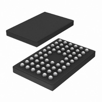
PTN3700EV/G,118 NXP Semiconductors, PTN3700EV/G,118 Datasheet - Page 30

PTN3700EV/G,118
Manufacturer Part Number
PTN3700EV/G,118
Description
IC MOBILE INTERFACE 56-VFBGA
Manufacturer
NXP Semiconductors
Type
Interfacer
Series
-r
Datasheet
1.PTN3700EVG118.pdf
(41 pages)
Specifications of PTN3700EV/G,118
Package / Case
56-VFBGA
Applications
Mobile Phones, Cellular, Video Displays
Mounting Type
Surface Mount
Input Current
4 uA
Maximum Operating Temperature
+ 85 C
Minimum Operating Temperature
- 40 C
Mounting Style
SMD/SMT
Operating Supply Voltage
1.8 V
Supply Voltage (max)
1.95 V
Supply Voltage (min)
1.65 V
Number Of Outputs
4
Lead Free Status / RoHS Status
Lead free / RoHS Compliant
Lead Free Status / RoHS Status
Lead free / RoHS Compliant, Lead free / RoHS Compliant
Other names
935284074118
PTN3700EV/G-T
PTN3700EV/G-T
PTN3700EV/G-T
PTN3700EV/G-T
Available stocks
Company
Part Number
Manufacturer
Quantity
Price
Company:
Part Number:
PTN3700EV/G,118
Manufacturer:
NXP Semiconductors
Quantity:
10 000
NXP Semiconductors
12. Application information
Table 23.
PTN3700_1
Product data sheet
Panel
QVGA
WQVGA
CIF+
HVGA
VGA
WVGA
SVGA
XGA
720p
Typical PCLK and number of data lanes
Horizontal
240
400
352
320
640
854
800
1024
1280
12.1 Typical lane and PCLK configurations
12.2 Pin configurations for various topologies of PCB
The PTN3700 supports PCLK (pixel clock) frequencies from 4 MHz to 65 MHz over 1, 2 or
3 data lanes.
overhead of 20 %. Note that 20 % overhead is an example value for illustration/calculation
purposes only and not a requirement.
There are two input pins, PSEL1 and PSEL0, on the PTN3700 that allow for pinning order
configurations.
PSEL1 will change the pinning order of the serial signals, and allow for various topologies
of PCB or flex layout without crossing the high-speed differential traces. The example
shown in
to avoid the traces crossing.
at receiver, and PSEL1 = 0 at transmitter.
PSEL0 can configure the pinning order of the parallel signals, and enables the easy
introduction of the PTN3700 into an existing parallel design avoiding board re-layout.
Figure 23
Vertical
320
240
416
480
480
480
600
768
720
Figure 23
and
Table 23
Color
bit
18
18
18
24
24
24
24
24
24
Figure 24
has set PSEL1 = 0 at receiver side, and PSEL1 = 1 at the transmitter
Other
bits
12
12
12
6
6
6
6
6
6
Rev. 01 — 14 August 2007
shows the typical number of data lanes needed, assuming blanking
show two configuration examples.
Figure 24
Frame
rate
(Hz)
60
60
60
60
60
60
60
60
60
Blanking
overhead
20 %
20 %
20 %
20 %
20 %
20 %
20 %
20 %
15 %
shows another configuration, which has PSEL1 = 1
1.8 V simple mobile interface link bridge IC
Pixel
clock
(MHz)
5.5
6.9
10.5
11.1
22.1
29.5
34.6
56.6
63.6
Serial aggregate data rate
(Mbit/s)
1-lane
165.9
207.4
316.3
331.8
PTN3700
2-lane
316.3
331.8
663.6
885.4
1036.8
© NXP B.V. 2007. All rights reserved.
3-lane
663.6
885.4
1036.8
1698.7
1909.7
30 of 41


