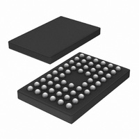
PTN3700EV/G,118 NXP Semiconductors, PTN3700EV/G,118 Datasheet - Page 2

PTN3700EV/G,118
Manufacturer Part Number
PTN3700EV/G,118
Description
IC MOBILE INTERFACE 56-VFBGA
Manufacturer
NXP Semiconductors
Type
Interfacer
Series
-r
Datasheet
1.PTN3700EVG118.pdf
(41 pages)
Specifications of PTN3700EV/G,118
Package / Case
56-VFBGA
Applications
Mobile Phones, Cellular, Video Displays
Mounting Type
Surface Mount
Input Current
4 uA
Maximum Operating Temperature
+ 85 C
Minimum Operating Temperature
- 40 C
Mounting Style
SMD/SMT
Operating Supply Voltage
1.8 V
Supply Voltage (max)
1.95 V
Supply Voltage (min)
1.65 V
Number Of Outputs
4
Lead Free Status / RoHS Status
Lead free / RoHS Compliant
Lead Free Status / RoHS Status
Lead free / RoHS Compliant, Lead free / RoHS Compliant
Other names
935284074118
PTN3700EV/G-T
PTN3700EV/G-T
PTN3700EV/G-T
PTN3700EV/G-T
Available stocks
Company
Part Number
Manufacturer
Quantity
Price
Company:
Part Number:
PTN3700EV/G,118
Manufacturer:
NXP Semiconductors
Quantity:
10 000
NXP Semiconductors
2. Features
3. Applications
1.
2.
PTN3700_1
Product data sheet
QVGA: 240
166 Mbit/s; 24-bit color data.
WVGA: 854
885.4 Mbit/s; 24-bit color data.
320 pixels at 60 Hz frame rate; 20 % non-active display data overhead; PCLK at 5.5 MHz; one-lane operation at
480 pixels at 60 Hz frame rate; 20 % non-active display data overhead; PCLK at 29.5 MHz; two-lane operation at
The PTN3700 automatically rotates the order of the essential signals (parallel CMOS and
high-speed serial data and clock) depending on whether it is operating as transmitter or as
receiver (using pin TX/RX). In addition, two Pinning Select bits (inputs PSEL[1:0]) allow for
four additional signal order configurations. This allows for various topologies of printed
circuit board or flex foil layout without crossing of traces; and enables the easy introduction
of PTN3700 into an existing ‘parallel’ design avoiding board re-layout.
The PTN3700 is available in a 56-ball VFBGA package and operates across a
temperature range of 40 C to +85 C.
I
I
I
I
I
I
I
I
I
I
I
I
I
I
I
Configurable as either Transmitter or Receiver
One of two serial transmission methods selectable (pixel clock referenced pseudo
source synchronous or bit clock referenced true source synchronous)
3 differential subLVDS high-speed serial lanes
One differential pixel clock
Configurable aggregate data bandwidth allowing up to 24-bit color, 60 fps XGA:
Parity encoding (transmitter) and detection (receiver) with last valid pixel repetition
Advanced Frame Mixing function (in Receiver mode) for 24-bit color depth using
conventional 18-bit displays or specially adapted ‘18-bit plus’ displays
Parallel CMOS I/O based on interface definition of RGB888 plus HS, VS, DE
Very low power profile:
Slew rate control on receiver parallel CMOS outputs
Operates from a single 1.8 V
Configurable mirroring pinout (dependent on Tx or Rx mode and PSEL[1:0] inputs) for
optimum single layer flex-foil flow-through in various application scenarios
Available in 56-ball VFBGA package
High-resolution mobile phones
Portable applications with video display capability
N
N
N
N
N
N
N
1 lane at 30 serialization rate up to 650 Mbit/s
2 lanes at 15 serialization rate up to 1300 Mbit/s
3 lanes at 10 serialization rate up to 1.95 Gbit/s
Shutdown mode for minimum idle power (< 3 A typical)
Low-power Standby mode with input clock frequency auto-detect (< 3 A typical)
Low active transmitter power: 18 mW (typ.) for QVGA
WVGA
Low active receiver power: 15 mW (typ.) for QVGA and 36 mW (typ.) for WVGA
2
Rev. 01 — 14 August 2007
150 mV power supply
1.8 V simple mobile interface link bridge IC
1
and 40 mW (typ.) for
PTN3700
© NXP B.V. 2007. All rights reserved.
2 of 41


