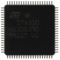
STA310 STMicroelectronics, STA310 Datasheet - Page 15

STA310
Manufacturer Part Number
STA310
Description
IC AUDIO DECODER 6+2CH 80-TQFP
Manufacturer
STMicroelectronics
Type
Audio Decoderr
Datasheet
1.STA310.pdf
(90 pages)
Specifications of STA310
Applications
HDTV, Players, Receivers, Set-Top Boxes
Voltage - Supply, Analog
2.5V
Voltage - Supply, Digital
2.5V
Mounting Type
Surface Mount
Package / Case
80-TQFP, 80-VQFP
Audio Codec Type
MP3 Decoder
No. Of Dacs
3
No. Of Input Channels
2
No. Of Output Channels
6
Adc / Dac Resolution
32bit
Sampling Rate
192kHz
Interface Type
I2C, Serial, Parallel
Rohs Compliant
Yes
Lead Free Status / RoHS Status
Lead free / RoHS Compliant
Other names
497-8856
STA310
STA310
Available stocks
Company
Part Number
Manufacturer
Quantity
Price
Part Number:
STA310
Manufacturer:
ST
Quantity:
20 000
Two independent inputs are available on the STA310.
The main one allows to enter input data stream through through:
The choice is performed by the register SIN_SETUP.
4.4.1 Data serial interface
When the serial mode is selected, the bitstreams can be entered into the STA310 through either:
The four-signal data interface (see Figure 5) provides:
Note: 1. Only 16-bit PCM streams are supported. For 20-bit or 24-bit PCM, the 4 or 8 least significant bits are ignored
.
The specifications of those signals can be configured by the means of the register CAN_SETUP.
Two modes exist in serial mode, one that uses the LRCLKIN pin and one that does not use the LRCLKIN pin.
4.4.1.1 Modes without the LRCLKIN pin
In this mode the signal LRCLKIN is not used by the STA310. The input data SIN is sampled on the rising edge
of DSTR. When the STA310 input buffer is full the REQ signal is asserted. The polarity of REQ signal is pro-
grammable through the register SIN_SETUP. The data must be sent most significant bits first.
When the decoder cannot accept further data the REQ is de-asserted and the DSTR clock must be stopped as
soon as possible to avoid data loss. After the REQ is de-asserted, the decoder is still able to accept data for a
limited number of clock cycles.
The maximum number of data that can be transmitted with respect to the change of REQ is given by the follow-
ing formula: Nbits = 23 - 6 * F
4.4.1.2 Modes using the LRCLKIN pin
When receiving data from an A/D converter or from an S/PDIF receiver, the signal LRCLKIN is used.
The LRCLKIN signal is used to make the distinction between the left and right channels. Any edge of the LR-
CLKIN signal indicates a word boundary.
The data transfer between the input interface and the FIFO is done on a byte basis. After the edge (rising or
falling) of the LRCLKIN, a new byte is transferred to the first stage of the STA310 every 8 DSTR clock cycles.
If the number of time slots is not a multiple of 8, the remaining data is lost. The polarity of LRCLKIN and DSTR
is programmable.
The LRCLKIN can be delayed by one time slot, in order to support PCM delayed mode. All these configurations
are programmable through the CAN_SETUP register.
The register CAN_SETUP has 4 significant bits, and each bit has a specific meaning, see
41.
Only the first byte is transferred to the STA310 because the number of time slots is 12 (8 + 4). SIN and LRCLKIN
are sampled on the falling edge of DSTR In this case SIN_SETUP = 3 and CAN_SETUP = LeftFirstChannel +
FallingStrobe + AllSlot = 2 + 4 + 8 = 14
- A serial interface (referred to as Data Serial Interface),
- And a parallel interface (referred to as Data Parallel Interface).
- a four-signal data interface or ,
- trough a SPDIF input (no external circuit is required).
- An input data line SIN,
- An input clock DSTR,
- A word clock input LRCLKIN
- And a hand-shake output signal REQ.
-
DSTR
/33MHz, where: F
DSTR
is the DSTR clock frequency, (max is 33 MHz).
CAN_SETUP on page
STA310
15/90


