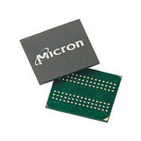
MT48H8M32LFB5-75 L:G Micron Technology Inc, MT48H8M32LFB5-75 L:G Datasheet - Page 52

MT48H8M32LFB5-75 L:G
Manufacturer Part Number
MT48H8M32LFB5-75 L:G
Description
Manufacturer
Micron Technology Inc
Type
Mobile SDRAMr
Datasheet
1.MT48H8M32LFB5-75_LG.pdf
(86 pages)
Specifications of MT48H8M32LFB5-75 L:G
Organization
8Mx32
Density
256Mb
Address Bus
14b
Access Time (max)
8/6ns
Maximum Clock Rate
133MHz
Operating Supply Voltage (typ)
1.8V
Package Type
VFBGA
Operating Temp Range
0C to 70C
Operating Supply Voltage (max)
1.95V
Operating Supply Voltage (min)
1.7V
Supply Current
100mA
Pin Count
90
Mounting
Surface Mount
Operating Temperature Classification
Commercial
Lead Free Status / Rohs Status
Compliant
- Current page: 52 of 86
- Download datasheet (3Mb)
Figure 22: Terminating a READ Burst
PDF: 09005aef834c13d2
256mb_mobile_sdram_y36n.pdf - Rev. I 11/09 EN
Note:
Continuous-page READ bursts can be truncated with a BURST TERMINATE command
and fixed-length READ bursts can be truncated with a BURST TERMINATE command,
provided that auto precharge was not activated. The BURST TERMINATE command
should be issued x cycles before the clock edge at which the last desired data element is
valid, where x = CL - 1. This is shown in Figure 22 (page 52) for each possible CAS
latency; data element n + 3 is the last desired data element of a longer burst.
Command
Command
1. DQM is LOW.
Address
Address
CLK
CLK
DQ
DQ
Bank,
T0
Col n
T0
READ
Bank,
READ
Col n
CL = 2
CL = 3
T1
T1
256Mb: 16 Meg x 16, 8 Meg x 32 Mobile SDRAM
NOP
NOP
52
T2
T2
NOP
NOP
D
OUT
Micron Technology, Inc. reserves the right to change products or specifications without notice.
T3
T3
NOP
NOP
D
D
OUT
OUT
TERMINATE
TERMINATE
BURST
BURST
T4
T4
X = 1 cycle
D
D
OUT
OUT
Transitioning data
X = 2 cycles
T5
T5
NOP
NOP
D
D
OUT
OUT
©2008 Micron Technology, Inc. All rights reserved.
T6
T6
READ Operation
NOP
NOP
D
OUT
Don’t Care
T7
NOP
Related parts for MT48H8M32LFB5-75 L:G
Image
Part Number
Description
Manufacturer
Datasheet
Request
R

Part Number:
Description:
IC SDRAM 64MBIT 133MHZ 54TSOP
Manufacturer:
Micron Technology Inc
Datasheet:

Part Number:
Description:
IC SDRAM 64MBIT 5.5NS 86TSOP
Manufacturer:
Micron Technology Inc
Datasheet:

Part Number:
Description:
IC SDRAM 64MBIT 200MHZ 86TSOP
Manufacturer:
Micron Technology Inc
Datasheet:

Part Number:
Description:
IC SDRAM 64MBIT 133MHZ 54TSOP
Manufacturer:
Micron Technology Inc
Datasheet:

Part Number:
Description:
IC SDRAM 128MBIT 133MHZ 54TSOP
Manufacturer:
Micron Technology Inc
Datasheet:

Part Number:
Description:
IC SDRAM 256MBIT 133MHZ 90VFBGA
Manufacturer:
Micron Technology Inc
Datasheet:

Part Number:
Description:
IC SDRAM 128MBIT 133MHZ 54TSOP
Manufacturer:
Micron Technology Inc
Datasheet:

Part Number:
Description:
IC SDRAM 256MBIT 133MHZ 54TSOP
Manufacturer:
Micron Technology Inc
Datasheet:

Part Number:
Description:
IC DDR SDRAM 512MBIT 6NS 66TSOP
Manufacturer:
Micron Technology Inc
Datasheet:

Part Number:
Description:
IC SDRAM 128MBIT 167MHZ 86TSOP
Manufacturer:
Micron Technology Inc
Datasheet:

Part Number:
Description:
IC SDRAM 128MBIT 143MHZ 86TSOP
Manufacturer:
Micron Technology Inc
Datasheet:

Part Number:
Description:
SDRAM 256M-BIT 1.8V 54-PIN VFBGA
Manufacturer:
Micron Technology Inc
Datasheet:

Part Number:
Description:
IC SDRAM 128MBIT 143MHZ 86TSOP
Manufacturer:
Micron Technology Inc
Datasheet:

Part Number:
Description:
IC SDRAM 128MBIT 125MHZ 54VFBGA
Manufacturer:
Micron Technology Inc
Datasheet:

Part Number:
Description:
IC SDRAM 128MBIT 125MHZ 54VFBGA
Manufacturer:
Micron Technology Inc
Datasheet:


