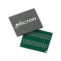
MT48H8M32LFB5-75 L:G Micron Technology Inc, MT48H8M32LFB5-75 L:G Datasheet - Page 40

MT48H8M32LFB5-75 L:G
Manufacturer Part Number
MT48H8M32LFB5-75 L:G
Description
Manufacturer
Micron Technology Inc
Type
Mobile SDRAMr
Datasheet
1.MT48H8M32LFB5-75_LG.pdf
(86 pages)
Specifications of MT48H8M32LFB5-75 L:G
Organization
8Mx32
Density
256Mb
Address Bus
14b
Access Time (max)
8/6ns
Maximum Clock Rate
133MHz
Operating Supply Voltage (typ)
1.8V
Package Type
VFBGA
Operating Temp Range
0C to 70C
Operating Supply Voltage (max)
1.95V
Operating Supply Voltage (min)
1.7V
Supply Current
100mA
Pin Count
90
Mounting
Surface Mount
Operating Temperature Classification
Commercial
Lead Free Status / Rohs Status
Compliant
Mode Register
Figure 13: Mode Register Definition
PDF: 09005aef834c13d2
256mb_mobile_sdram_y36n.pdf - Rev. I 11/09 EN
Mn+2 Mn+1
0
0
1
1
0
1
0
1
Mn+2
n+2 n+1
0
Mode Register Definition
Base mode register
Reserved
Extended mode register
Reserved
BA1
M9
0
1
Mn+1
The mode register defines the specific mode of operation, including burst length (BL),
burst type, CAS latency (CL), operating mode, and write burst mode. The mode register
is programmed via the LOAD MODE REGISTER command and retains the stored infor-
mation until it is programmed again or the device loses power.
Mode register bits M[2:0] specify the BL; M3 specifies the type of burst; M[6:4] specify
the CL; M7 and M8 specify the operating mode; M9 specifies the write burst mode; and
M10–Mn should be set to zero to ensure compatibility with future revisions. Mn + 1 and
Mn + 2 should be set to zero to select the mode register.
The mode registers must be loaded when all banks are idle, and the controller must
wait
ments will result in unspecified operation.
0
Programmed burst length
Single location access
BA0
M8
0
–
Write Burst Mode
An
Mn
t
n
Reserved*
MRD before initiating the subsequent operation. Violating either of these require-
M7
0
–
...
...
...
Normal operation
All other states reserved
Operating Mode
10
A10
M10
WB
M6
0
0
0
0
1
1
1
1
A9
M9
9
Op mode
M5
0
0
1
1
0
0
1
1
M8
A8
8
256Mb: 16 Meg x 16, 8 Meg x 32 Mobile SDRAM
M4
0
1
0
1
0
1
0
1
A7
M7
7
CAS Latency
CAS latency
40
M6
A6
6
Reserved
Reserved
Reserved
Reserved
Reserved
Reserved
2
3
5
A5
M5
M4
4
A4
Micron Technology, Inc. reserves the right to change products or specifications without notice.
BT
M3
A3
3
M2
Burst length
0
0
0
0
1
1
1
1
A2
M2
2
M1
*Should be programmed to 0
0
0
1
1
0
0
1
1
to ensure compatibility
with future devices.
M1
1
A1
M3
M0
0
1
0
1
0
1
0
1
0
1
M0
A0
0
Continuous
Reserved
Reserved
Reserved
M3 = 0
Interleaved
Burst Type
Sequential
1
2
4
8
Address bus
Mode
register (Mx)
Burst Length
©2008 Micron Technology, Inc. All rights reserved.
Reserved
Reserved
Reserved
Reserved
Mode Register
M3 = 1
1
2
4
8


