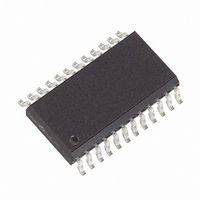
MAX191BCWG+ Maxim Integrated Products, MAX191BCWG+ Datasheet - Page 7

MAX191BCWG+
Manufacturer Part Number
MAX191BCWG+
Description
IC ADC 12BIT 100KSPS W/REF24SOIC
Manufacturer
Maxim Integrated Products
Datasheet
1.MAX191BCWG.pdf
(24 pages)
Specifications of MAX191BCWG+
Number Of Bits
12
Sampling Rate (per Second)
100k
Data Interface
MICROWIRE™, Parallel, QSPI™, Serial, SPI™
Number Of Converters
1
Power Dissipation (max)
941mW
Voltage Supply Source
Dual ±
Operating Temperature
0°C ~ 70°C
Mounting Type
Surface Mount
Package / Case
24-SOIC (0.300", 7.50mm Width)
Number Of Adc Inputs
1
Architecture
SAR
Conversion Rate
100 KSPs
Resolution
12 bit
Input Type
Differential
Interface Type
3-Wire (SPI, QSPI, MICROWIRE)
Supply Voltage (max)
5 V
Maximum Power Dissipation
1067 mW
Maximum Operating Temperature
+ 70 C
Mounting Style
SMD/SMT
Minimum Operating Temperature
0 C
Lead Free Status / RoHS Status
Lead free / RoHS Compliant
PIN
10
11
12
13
14
15
16
17
18
19
20
21
22
23
24
1
2
3
4
5
6
7
8
9
D6/SCLK
CLK/SCLK
D7/DOUT
D5/SSTRB
REFADJ
D2/D10
D3/D11
NAME
DGND
AGND
D0/D8
D1/D9
HBEN
BUSY
VREF
AIN+
AIN-
PAR
V
V
BIP
RD
PD
D4
CS
DD
SS
OUT
with Internal Reference and Power-Down
_______________________________________________________________________________________
Power-Down Input. A logic low at PD deactivates the ADC—only the bandgap reference is active. A logic
high selects normal operation, internal-reference compensation mode. An open-circuit condition selects
normal operation, external-reference compensation mode.
Negative Supply, 0V to -5.25V
Sampled Analog Input
Analog Input Return. Pseudo-differential (see Gain and Offset Adjustment section).
Reference-Buffer Output for Internal Reference. Input for external reference when REFADJ is connected to
V
Reference Adjust. Connect to V
Analog Ground
BIP = low selects unipolar mode
BIP = high selects bipolar mode (see Gain and Offset Adjustment section)
BUSY Output is low during a conversion.
Three-State Data Outputs: LSB = D0
Three-State Data Outputs
Digital Ground
Three-State Data Outputs
Three-State Data Outputs: MSB = D11
Three-State Data Output
Three-State Data Output/Serial Strobe Output in serial mode
Three-State Data Output/Serial Clock Output in serial mode
Three-State Data Output/Data Output in serial mode
Read Input. In parallel mode, a low signal starts a conversion when CS and HBEN are low (memory
mode). RD also enables the outputs when CS is low. In serial mode, RD = low enables SCLK
SSTRB when CS is low. RD = high forces SCLK
Chip-Select Input must be low for the ADC to recognize RD and HBEN inputs in parallel mode. The falling
edge of CS starts a conversion in serial mode. CS = high in serial mode forces SCLK
DOUT into a high-impedance state.
High-Byte Enable Input. In parallel mode, HBEN = high multiplexes the 4 MSBs of the conversion result
into the lower bit outputs. HBEN = high also disables conversion starts. HBEN = low places the 8 LSBs
onto the data bus. In serial mode, HBEN = low enables SCLK
HBEN = high enables SCLK
Sets the output mode. PAR = high selects parallel output mode. PAR = low selects serial output mode.
Clock Input/Serial Clock Input in serial mode. An external TTL-/CMOS-compatible clock may be applied to
this pin, or a capacitor (120pF nominal) may be connected between CLK and DGND to operate the internal
oscillator.
Positive Supply, +5V ±5%
DD
.
Low-Power, 12-Bit Sampling ADC
OUT
DD
to operate continuously, provided CS is low.
to use an extended reference at VREF.
FUNCTION
OUT
and SSTRB into a high-impedance state.
OUT
to operate during the conversion only,
Pin Description
OUT
, SSTRB, and
OUT
and
7


