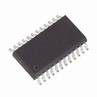
MAX191BCWG+ Maxim Integrated Products, MAX191BCWG+ Datasheet - Page 10

MAX191BCWG+
Manufacturer Part Number
MAX191BCWG+
Description
IC ADC 12BIT 100KSPS W/REF24SOIC
Manufacturer
Maxim Integrated Products
Datasheet
1.MAX191BCWG.pdf
(24 pages)
Specifications of MAX191BCWG+
Number Of Bits
12
Sampling Rate (per Second)
100k
Data Interface
MICROWIRE™, Parallel, QSPI™, Serial, SPI™
Number Of Converters
1
Power Dissipation (max)
941mW
Voltage Supply Source
Dual ±
Operating Temperature
0°C ~ 70°C
Mounting Type
Surface Mount
Package / Case
24-SOIC (0.300", 7.50mm Width)
Number Of Adc Inputs
1
Architecture
SAR
Conversion Rate
100 KSPs
Resolution
12 bit
Input Type
Differential
Interface Type
3-Wire (SPI, QSPI, MICROWIRE)
Supply Voltage (max)
5 V
Maximum Power Dissipation
1067 mW
Maximum Operating Temperature
+ 70 C
Mounting Style
SMD/SMT
Minimum Operating Temperature
0 C
Lead Free Status / RoHS Status
Lead free / RoHS Compliant
between 45% and 55%.
For best analog performance on the MAX191, the clock
should be synchronized to the conversion start signals
(CS and RD) as shown in Figure 6. A conversion should
not be started in the 50ns before a clock edge nor in
the 100ns after it. This ensures that CLK transitions are
not coupled to the analog input and sampled by the
T/H. The magnitude of this feedthrough can be a few
millivolts. When the clock and conversion start signals
are synchronized, small end-point errors (offset and
full-scale) are the most that can be generated by clock
feedthrough. Even these errors (which can be trimmed
out) can be avoided by ensuring that the start of a con-
version (RD or CS falling edge) does not occur close to
a clock transition (Figure 6), as described above.
The data output from the MAX191 is straight binary in
the unipolar mode. In the bipolar mode, the MSB is
inverted (see Figure 22). The 12 data bits can be out-
put either in two 8-bit bytes or as a serial output. Table
1 shows the data-bus output format.
A 2-byte read uses outputs D7–D0. Byte selection is
controlled by HBEN. When HBEN is low, the lower 8
bits appear at the data outputs. When HBEN is high,
the upper 4 bits appear at D0-D3 with the leading 4 bits
low in locations D4–D7.
Conversion-start and data-read operations are con-
trolled by the HBEN, CS, and RD digital inputs. A logic
low is required on all three inputs to start a conversion,
and once the conversion is in progress it cannot be
Low-Power, 12-Bit Sampling ADC
with Internal Reference and Power-Down
Figure 6.
10
CS + RD
BUSY
CLK
______________________________________________________________________________________
CS, RD, and CLK Synchronous Operation
Clock and Control Synchronization
t
16
Parallel Digital-Interface Mode
t
2
t
17
t
2
Output-Data Format
Timing and Control
restarted. BUSY remains low during the entire conver-
sion cycle.
The timing diagrams of Figures 7–10 outline two paral-
lel-interface modes and one serial mode.
In slow-memory mode, the device appears to the µP as
a slow peripheral or memory. Conversion is initiated
with a read instruction (see Figure 7 and Table 2). Set
the PAR pin high for parallel interface mode. Beginning
with HBEN low, taking CS and RD low starts the con-
version. The analog input is sampled on the falling
edge of RD. BUSY remains low while the conversion is
in progress. The previous conversion result appears at
the digital outputs until the end of conversion, when
BUSY returns high. The output latches are then updat-
ed with the newest results of the 8 LSBs on D7–D0. A
second read operation with HBEN high places the 4
MSBs, with 4 leading 0s, on data outputs D7–D0. The
second read operation does not start a new conversion
because HBEN is high.
As in slow-memory mode, D7–D0 are used for 2-byte
reads. A conversion starts with a read instruction with
HBEN and CS low. The T/H samples the input on the
falling edge of RD (see Figure 8 and Table 3). PAR is set
high. At this point the data outputs contain the 8 LSBs
from the previous conversion. Two more read operations
are needed to access the conversion result. The first
occurs with HBEN high, where the 4 MSBs with 4 leading
0s are accessed. The second read, with HBEN low, out-
puts the 8 LSBs and also starts a new conversion.
Figure 9 and Table 4 show how to read output data
within one conversion cycle without starting another
conversion. Trigger the falling edge of a read on the ris-
t
t
CONV
CONV
Slow-Memory Mode
ROM Mode
t
13


