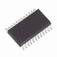
MAX191BCWG+ Maxim Integrated Products, MAX191BCWG+ Datasheet - Page 2

MAX191BCWG+
Manufacturer Part Number
MAX191BCWG+
Description
IC ADC 12BIT 100KSPS W/REF24SOIC
Manufacturer
Maxim Integrated Products
Datasheet
1.MAX191BCWG.pdf
(24 pages)
Specifications of MAX191BCWG+
Number Of Bits
12
Sampling Rate (per Second)
100k
Data Interface
MICROWIRE™, Parallel, QSPI™, Serial, SPI™
Number Of Converters
1
Power Dissipation (max)
941mW
Voltage Supply Source
Dual ±
Operating Temperature
0°C ~ 70°C
Mounting Type
Surface Mount
Package / Case
24-SOIC (0.300", 7.50mm Width)
Number Of Adc Inputs
1
Architecture
SAR
Conversion Rate
100 KSPs
Resolution
12 bit
Input Type
Differential
Interface Type
3-Wire (SPI, QSPI, MICROWIRE)
Supply Voltage (max)
5 V
Maximum Power Dissipation
1067 mW
Maximum Operating Temperature
+ 70 C
Mounting Style
SMD/SMT
Minimum Operating Temperature
0 C
Lead Free Status / RoHS Status
Lead free / RoHS Compliant
ABSOLUTE MAXIMUM RATINGS
ELECTRICAL CHARACTERISTICS
(V
mode, reference compensation mode—external, synchronous operation, Figure 6, T
Low-Power, 12-Bit Sampling ADC
with Internal Reference and Power-Down
V
V
V
AGND, VREF, REFADJ to DGND................-0.3V to (V
AIN+, AIN-,
CS, RD, CLK, BIP, HBEN, PAR, to DGND....-0.3V to (V
BUSY, D0–D7 to DGND..............................-0.3V to (V
Continuous Power Dissipation (T
Stresses beyond those listed under “Absolute Maximum Ratings" may cause permanent damage to the device. These are stress ratings only, and functional
operation of the device at these or any other conditions beyond those indicated in the operational sections of the specifications is not implied. Exposure to
absolute maximum rating conditions for extended periods may affect device reliability.
2
Wide SO (derate 11.76mW/°C above +70°C) ......................941mW
Narrow CERDIP (derate 12.50mW/°C above +70°C) ........1000mW
Resolution
Integral Nonlinearity
Narrow Plastic DIP (derate 13.33mW/°C above +70°C)....1067mW
DC ACCURACY (Note 2)
DYNAMIC ACCURACY (sample rate = 100kHz, V
CONVERSION RATE
DD
SS
DD
Differential Nonlinearity
Offset Error
Gain Error (Note 3)
Gain-Error Tempco (Note 4)
Signal-to-Noise plus Distortion
Ratio
Total Harmonic Distortion
(up to the 5th Harmonic)
Spurious-Free Dynamic Range
Conversion Time (Note 5)
Track/Hold Acquisition Time
Aperture Delay
Aperture Jitter
External Clock Frequency
Range (Note 6)
DD
_______________________________________________________________________________________
to AGND ............................................................-7V to +0.3V
to DGND............................................................-0.3V to +7V
to V
= 5V ±5%, V
SS
PARAMETER
..............................................................................12V
PD to V
SS
SS
= 0V or -5V ±5%, f
.................................-0.3V to (V
A
= +70°C)
SYMBOL
CLK
SINAD
SFDR
t
DNL
THD
CONV
f
INL
CLK
= 1.6MHz, 50% duty cycle, AIN- = AGND, BIP = 0V, slow-memory mode, internal-reference
MAX191A
MAX191B
No missing codes over temperature
MAX191A
MAX191B
MAX191A
MAX191B
Excludes internal-reference drift
IN
1kHz input signal, T
1kHz input signal, T
1kHz input signal, T
Synchronous CLK (12 to 13 CLKs)
Internal CLK, C
DD
DD
DD
DD
= 4Vp-p)
+ 0.3V)
+ 0.3V)
+ 0.3V)
+ 0.3V)
CONDITIONS
L
= 120pF
Operating Temperature Ranges
Storage Temperature Range.....................................-65°C to +160°C
Lead Temperature (soldering, 10sec).....................................+300°C
MAX191_C_ _ ................................................................0°C to +70°C
MAX191_E_ _ .............................................................-40°C to +85°C
MAX191_M_ _ ..........................................................-55°C to +125°C
A
A
A
= +25°C
= +25°C
= +25°C
A
= T
MIN
to T
MAX
7.50
MIN
, unless otherwise noted.) (Note 1)
0.1
12
70
80
6
±0.2
TYP
12
25
50
8.125
MAX
±1/2
-80
1.6
±1
±1
±1
±2
±2
±3
18
2
ppm/°C
UNITS
MHz
LSB
LSB
LSB
LSB
Bits
dB
dB
dB
µs
µs
ns
ps


