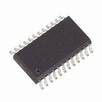
MAX191BCWG+ Maxim Integrated Products, MAX191BCWG+ Datasheet - Page 5

MAX191BCWG+
Manufacturer Part Number
MAX191BCWG+
Description
IC ADC 12BIT 100KSPS W/REF24SOIC
Manufacturer
Maxim Integrated Products
Datasheet
1.MAX191BCWG.pdf
(24 pages)
Specifications of MAX191BCWG+
Number Of Bits
12
Sampling Rate (per Second)
100k
Data Interface
MICROWIRE™, Parallel, QSPI™, Serial, SPI™
Number Of Converters
1
Power Dissipation (max)
941mW
Voltage Supply Source
Dual ±
Operating Temperature
0°C ~ 70°C
Mounting Type
Surface Mount
Package / Case
24-SOIC (0.300", 7.50mm Width)
Number Of Adc Inputs
1
Architecture
SAR
Conversion Rate
100 KSPs
Resolution
12 bit
Input Type
Differential
Interface Type
3-Wire (SPI, QSPI, MICROWIRE)
Supply Voltage (max)
5 V
Maximum Power Dissipation
1067 mW
Maximum Operating Temperature
+ 70 C
Mounting Style
SMD/SMT
Minimum Operating Temperature
0 C
Lead Free Status / RoHS Status
Lead free / RoHS Compliant
TIMING CHARACTERISTICS (Figures 6–10) (continued)
(V
Note 1:
Note 2:
Note 3:
Note 4:
Note 5:
Note 6:
Note 7:
Note 8:
Note 9:
Note 10: REFADJ adjustment range is defined as the allowed voltage excursion on REFADJ relative to its unadjusted value of 2.4V.
Note 11: This current is included in the PD supply current specification.
Note 12: Floating the PD pin guarantees external compensation mode.
Note 13: V
Note 14: All input control signals are specified with t
Note 15: t
Note 16: t
CS or RD Hold Time
CS or RD Setup Time
CS to DOUT Three-State
SCLK to SCLK
SCLK
SCLK to DOUT Delay
SCLK to SSTRB Delay
DD
=5V ±5%, V
OUT
PARAMETER
Performance at power-supply tolerance limits guaranteed by power-supply rejection test.
V
FS = VREF, offset nulled, ideal last-code transition = FS - 3/2 LSB.
Gain-Error Tempco = ∆GE is the gain-error change from T
Conversion time defined as the number of clock cycles times the clock period; clock has a 50% duty cycle.
Guaranteed by design, not production tested.
AIN+, AIN- must not exceed supplies for specified accuracy.
VREF TC = ∆T, where ∆VREF is reference-voltage change from T
Output current should not change during conversion. This current is in addition to the current required by the internal DAC.
This will typically result in a 1.7 times larger change in the REF output (Figure 19a).
3
7
to DOUT Delay
DD
REF
and t
is defined as the time required for the data lines to change 0.5V when loaded with the circuits of Figure 2.
= 5V, V
OUT
= 4.096V, external reference.
SS
6
with Internal Reference and Power-Down
are measured with the load circuits of Figure 1 and defined as the time required for an output to cross 0.8V or 2.4V.
= 0V or -5V ±5%, T
Delay
_______________________________________________________________________________________
SS
= 0V, FS = VREF.
SYMBOL
t
t
t
t
t
t
t
16
17
19
20
21
22
23
A
= T
Low-Power, 12-Bit Sampling ADC
CONDITIONS
MIN
to T
MAX
r
= t
, unless otherwise noted.) (Note 14)
f
= 5ns (10% to 90% of 5V) and timed from a voltage level of 1.6V.
MIN
150
10
T
A
= +25°C
TYP MAX
A
= +25°C to T
100
160
100
240
260
A
= +25°C to T
MIN
MIN
150
10
MAX191C/E
or T
TYP MAX
MIN
MAX
or T
.
110
180
130
260
310
MAX
.
MIN
150
10
MAX191M
TYP MAX
120
200
150
280
350
UNITS
ns
ns
ns
ns
ns
ns
ns
5


