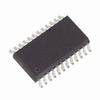
MAX191BCWG+ Maxim Integrated Products, MAX191BCWG+ Datasheet - Page 22

MAX191BCWG+
Manufacturer Part Number
MAX191BCWG+
Description
IC ADC 12BIT 100KSPS W/REF24SOIC
Manufacturer
Maxim Integrated Products
Datasheet
1.MAX191BCWG.pdf
(24 pages)
Specifications of MAX191BCWG+
Number Of Bits
12
Sampling Rate (per Second)
100k
Data Interface
MICROWIRE™, Parallel, QSPI™, Serial, SPI™
Number Of Converters
1
Power Dissipation (max)
941mW
Voltage Supply Source
Dual ±
Operating Temperature
0°C ~ 70°C
Mounting Type
Surface Mount
Package / Case
24-SOIC (0.300", 7.50mm Width)
Number Of Adc Inputs
1
Architecture
SAR
Conversion Rate
100 KSPs
Resolution
12 bit
Input Type
Differential
Interface Type
3-Wire (SPI, QSPI, MICROWIRE)
Supply Voltage (max)
5 V
Maximum Power Dissipation
1067 mW
Maximum Operating Temperature
+ 70 C
Mounting Style
SMD/SMT
Minimum Operating Temperature
0 C
Lead Free Status / RoHS Status
Lead free / RoHS Compliant
0.01µF and 10µF bypass capacitors. Minimize capaci-
tor lead lengths for best supply-noise rejection. If the
+5V power supply is very noisy, a 10Ω resistor can be
connected as a lowpass filter to filter out supply noise
(Figure 23).
High-speed sampling capability and throughput make
the MAX191 ideal for wideband signal processing. To
support these and other related applications, Fast
Fourier Transform (FFT) test techniques guarantee the
ADC's dynamic frequency response, distortion, and
noise at the rated throughput. Specifically, this involves
applying a low-distortion sine wave to the ADC input
and recording the digital conversion results for a speci-
fied time. The data is then analyzed using an FFT algo-
rithm, which determines its spectral content.
Conversion errors are then seen as spectral elements
outside the fundamental input frequency. FFT plots are
shown in the Typical Operating Characteristics .
ADCs have traditionally been evaluated by specifica-
tions such as zero and full-scale error, integral nonlin-
earity (INL), and differential nonlinearity (DNL). Such
parameters are widely accepted for specifying perfor-
mance with DC and slowly varying signals, but are less
useful in signal-processing applications where the
ADC’s impact on the system transfer function is the
main concern. The significance of various DC errors
does not translate well to the dynamic case, so different
tests are required.
Signal-to-Noise Ratio (SNR) is the ratio between the
RMS amplitude of the fundamental input frequency to
the RMS amplitude of all other A/D output signals,
except signal harmonics. Signal-to-Noise + Distortion
ratio (SINAD) is the same as the SNR, but includes sig-
nal harmonics.
Low-Power, 12-Bit Sampling ADC
with Internal Reference and Power-Down
22
_____________Dynamic Performance
______________________________________________________________________________________
The theoretical minimum A/D noise is caused by quan-
tization error and is a direct result of the ADC’s resolu-
tion: SNR = (6.02n + 1.76) dB, where n is the number of
bits of resolution. 74dB is the SNR of a perfect 12-bit
ADC.
By transposing the equation that converts resolution to
SNR we can compute the effective resolution or the
“effective number of bits” the ADC provides from the
measured SNR:
Total Harmonic Distortion (THD) is the ratio of the RMS
sum of all harmonics of the input signal (in the frequen-
cy band above DC and below one-half the sample rate)
to the fundamental itself. This expressed as:
THD = 20log
where V
V
Spurious-free dynamic range is the ratio of the funda-
mental RMS amplitude to the amplitude of the next
largest spectral component (in the frequency band
above DC and below one-half the sample rate). Usually
this peak occurs at some harmonic of the input fre-
quency. But if the ADC is exceptionally linear, it can
occur at a random peak in the ADC’s noise floor.
Many industrial applications require isolation to prevent
excessive current flow where ground disparities exist
between the ADC and the rest of the system. In Figure
24, a MAX250 and four 6N136 opto-couplers create an
n
are the amplitudes of the 2nd through n
1
n = (SNR – 1.76)/6.02
is the fundamental RMS amplitude and V
[
√(V
Spurious-Free Dynamic Range
2
2
+ V
Opto-Isolated A/D Interface
Total Harmonic Distortion
3
2
+ V
4
2
+ V
5
2
+ . . . + V
th
harmonics.
n
2
) /V
1
2
]
to


