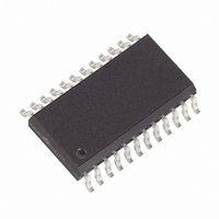
MAX191BCWG+ Maxim Integrated Products, MAX191BCWG+ Datasheet - Page 21

MAX191BCWG+
Manufacturer Part Number
MAX191BCWG+
Description
IC ADC 12BIT 100KSPS W/REF24SOIC
Manufacturer
Maxim Integrated Products
Datasheet
1.MAX191BCWG.pdf
(24 pages)
Specifications of MAX191BCWG+
Number Of Bits
12
Sampling Rate (per Second)
100k
Data Interface
MICROWIRE™, Parallel, QSPI™, Serial, SPI™
Number Of Converters
1
Power Dissipation (max)
941mW
Voltage Supply Source
Dual ±
Operating Temperature
0°C ~ 70°C
Mounting Type
Surface Mount
Package / Case
24-SOIC (0.300", 7.50mm Width)
Number Of Adc Inputs
1
Architecture
SAR
Conversion Rate
100 KSPs
Resolution
12 bit
Input Type
Differential
Interface Type
3-Wire (SPI, QSPI, MICROWIRE)
Supply Voltage (max)
5 V
Maximum Power Dissipation
1067 mW
Maximum Operating Temperature
+ 70 C
Mounting Style
SMD/SMT
Minimum Operating Temperature
0 C
Lead Free Status / RoHS Status
Lead free / RoHS Compliant
Figure 21b. Offset (±10mV) and Gain (±1%) Trim Circuit
Wire-wrap boards are not recommended. Board layout
should ensure that digital- and analog-signal lines are
separated from each other. Do not run analog and digi-
tal (especially clock) lines parallel to one another, or
digital lines underneath the ADC package.
Figure 23 shows the recommended system ground
connections. Establish a single-point ground (“star”
ground point) at AGND, separate from the logic
ground. Connect all other analog grounds and DGND
to it. No other digital-system ground should be con-
nected to this single-point analog ground. The ground
return to the power supply for this star ground should
be low impedance and as short as possible for noise-
free operation.
High-frequency noise in the V
affect the high-speed comparator in the ADC. Bypass
these supplies to the single-point analog ground with
V
* CONNECT AIN- TO AGND WHEN USING DUAL SUPPLIES
IN
10k
R7
10k
R8
10k
R6
VREF
with Internal Reference and Power-Down
0.1 F*
______________________________________________________________________________________
MAX480
10k
R5
100
10k
10k
R9*
20k
R1
R2
R3
49.9
VREF
R4
49.9
DD
R10*
power supply may
Low-Power, 12-Bit Sampling ADC
AIN -
AIN +
MAX191
D0–D11
Figure 22. Bipolar Transfer Function
Figure 23. Power-Supply Grounding Connection
SINGLE SUPPLY
DUAL SUPPLY
AIN- = 0V
(
AIN- = ––––
*OPTIONAL
01 . . . 111
01 . . . 110
00 . . . 010
00 . . . 001
00 . . . 000
11 . . . 111
11 . . . 110
11 . . . 101
10 . . . 001
10 . . . 000
V
+5V
DD
VREF
2
R* = 10
)
-VREF
––––
0V
2
AGND
MAX191
SUPPLIES
V
-5V
SS
DGND
––––
VREF
0V
2
+5V
CIRCUITRY
DIGITAL
–––– - 1LSB
VREF
DGND
VREF - 1LSB
GND
2
21


