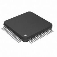
DS3106LN+ Maxim Integrated Products, DS3106LN+ Datasheet - Page 74

DS3106LN+
Manufacturer Part Number
DS3106LN+
Description
IC TIMING LINE CARD 64-LQFP
Manufacturer
Maxim Integrated Products
Type
Timing Card ICr
Datasheet
1.DS3106LN.pdf
(87 pages)
Specifications of DS3106LN+
Input
CMOS, LVDS, LVPECL, TTL
Output
CMOS, LVDS, LVPECL, TTL
Frequency - Max
312.5MHz
Voltage - Supply
1.62 V ~ 1.98 V
Operating Temperature
-40°C ~ 85°C
Mounting Type
Surface Mount
Package / Case
64-LQFP
Frequency-max
312.5MHz
Lead Free Status / RoHS Status
Lead free / RoHS Compliant
- Current page: 74 of 87
- Download datasheet (499Kb)
____________________________________________________________________________________________ DS3106
9.4
JTAG Test Registers
IEEE 1149.1 requires a minimum of two test registers—the bypass register and the boundary scan register. An
optional test register, the identification register, has been included in the device design. It is used with the IDCODE
instruction and the Test-Logic-Reset state of the TAP controller.
Bypass Register. This is a single 1-bit shift register used with the BYPASS, CLAMP, and HIGHZ instructions to
provide a short path between JTDI and JTDO.
Boundary Scan Register. This register contains a shift register path and a latched parallel output for control cells
and digital I/O cells. BSDL files are available at www.maxim-ic.com/TechSupport/telecom/bsdl.htm.
Identification Register. This register contains a 32-bit shift register and a 32-bit latched parallel output. It is
selected during the IDCODE instruction and when the TAP controller is in the Test-Logic-Reset state. The device
identification code for the DS3106 is shown in
Table
9-2.
Table 9-2. JTAG ID Code
DEVICE
REVISION
DEVICE CODE
MANUFACTURER CODE
REQUIRED
DS3106
Consult factory
00010100001
1
0000000010100100
19-4629; Rev 4; 8/10
74 of 87
Related parts for DS3106LN+
Image
Part Number
Description
Manufacturer
Datasheet
Request
R

Part Number:
Description:
Ds3106 - New! - Line Card Timing Ic
Manufacturer:
Maxim Integrated Products, Inc.
Datasheet:

Part Number:
Description:
MAX7528KCWPMaxim Integrated Products [CMOS Dual 8-Bit Buffered Multiplying DACs]
Manufacturer:
Maxim Integrated Products
Datasheet:

Part Number:
Description:
Single +5V, fully integrated, 1.25Gbps laser diode driver.
Manufacturer:
Maxim Integrated Products
Datasheet:

Part Number:
Description:
Single +5V, fully integrated, 155Mbps laser diode driver.
Manufacturer:
Maxim Integrated Products
Datasheet:

Part Number:
Description:
VRD11/VRD10, K8 Rev F 2/3/4-Phase PWM Controllers with Integrated Dual MOSFET Drivers
Manufacturer:
Maxim Integrated Products
Datasheet:

Part Number:
Description:
Highly Integrated Level 2 SMBus Battery Chargers
Manufacturer:
Maxim Integrated Products
Datasheet:

Part Number:
Description:
Current Monitor and Accumulator with Integrated Sense Resistor; ; Temperature Range: -40°C to +85°C
Manufacturer:
Maxim Integrated Products

Part Number:
Description:
TSSOP 14/A�/RS-485 Transceivers with Integrated 100O/120O Termination Resis
Manufacturer:
Maxim Integrated Products

Part Number:
Description:
TSSOP 14/A�/RS-485 Transceivers with Integrated 100O/120O Termination Resis
Manufacturer:
Maxim Integrated Products

Part Number:
Description:
QFN 16/A�/AC-DC and DC-DC Peak-Current-Mode Converters with Integrated Step
Manufacturer:
Maxim Integrated Products

Part Number:
Description:
TDFN/A/65V, 1A, 600KHZ, SYNCHRONOUS STEP-DOWN REGULATOR WITH INTEGRATED SWI
Manufacturer:
Maxim Integrated Products

Part Number:
Description:
Integrated Temperature Controller f
Manufacturer:
Maxim Integrated Products

Part Number:
Description:
SOT23-6/I�/45MHz to 650MHz, Integrated IF VCOs with Differential Output
Manufacturer:
Maxim Integrated Products

Part Number:
Description:
SOT23-6/I�/45MHz to 650MHz, Integrated IF VCOs with Differential Output
Manufacturer:
Maxim Integrated Products

Part Number:
Description:
EVALUATION KIT/2.4GHZ TO 2.5GHZ 802.11G/B RF TRANSCEIVER WITH INTEGRATED PA
Manufacturer:
Maxim Integrated Products


