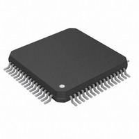
DS3106LN+ Maxim Integrated Products, DS3106LN+ Datasheet - Page 25

DS3106LN+
Manufacturer Part Number
DS3106LN+
Description
IC TIMING LINE CARD 64-LQFP
Manufacturer
Maxim Integrated Products
Type
Timing Card ICr
Datasheet
1.DS3106LN.pdf
(87 pages)
Specifications of DS3106LN+
Input
CMOS, LVDS, LVPECL, TTL
Output
CMOS, LVDS, LVPECL, TTL
Frequency - Max
312.5MHz
Voltage - Supply
1.62 V ~ 1.98 V
Operating Temperature
-40°C ~ 85°C
Mounting Type
Surface Mount
Package / Case
64-LQFP
Frequency-max
312.5MHz
Lead Free Status / RoHS Status
Lead free / RoHS Compliant
7.8.1 Signal Format Configuration
Output clock OC6 is an LVDS-compatible, LVPECL level-compatible outputs. The type of output can be selected or
the output can be disabled using the OC6SF configuration bits in the
mode generates a differential signal that is large enough for most LVPECL receivers. Some LVPECL receivers
have a limited common-mode signal range that can be accommodated for by using an AC-coupled signal. The
LVDS electrical specifications are listed in
10-1. The LVPECL level-compatible electrical specifications are listed in
LVPECL receiver termination is shown in
LVPECL, and CML inputs on neighboring ICs using a few external passive components. See
HFAN-1.0
Output clocks OC3, FSYNC, and MFSYNC are CMOS/TTL signal format.
7.8.2 Frequency Configuration
The frequency of output clocks OC3 and OC6 is a function of the settings used to configure the components of the
T0 PLL paths. These components are shown in the detailed block diagram of
The DS3106 uses digital frequency synthesis (DFS) to generate various clocks. In DFS a high-speed master clock
(204.8MHz) is divided down to the desired output frequency by adding a number to an accumulator. The DFS
output is a coding of the clock output phase that is used by a special circuit to determine where to put the edges of
the output clock between the clock edges of the master clock. The edges of the output clock, however, are not
ideally located in time, resulting in jitter with an amplitude typically less than 1ns pk-pk.
7.8.2.1 T0 DPLL and Feedback DFS Details
See
internal clocks from which the output and feedback clocks are derived.
The feedback DFS block synthesizes the appropriate locking frequencies for use by the phase-frequency detector
(PFD). See Section 7.4.2.
7.8.2.2 Output DFS and APLL Details
See
blocks, and three APLL DFS blocks. The T0 APLL, the T0 APLL2, and the T4 APLL (and their output dividers) get
their frequency references from three associated APLL DFS blocks. All the output DFS blocks are connected to the
T0 DPLL.
The 2K8K DFS and FSYNC DFS blocks generate both 2kHz and 8kHz signals, which have about 1ns pk-pk jitter.
The FSYNC (8kHz) and MFSYNC (2 kHz) signals come from the FSYNC DFS block. The 2kHz and 8 kHz signals
that can be output on OC3 or OC6 always come from the 2K8K DFS.
The DIG1 DFS can generate an N x DS1 or N x E1 signal with about 1ns pk-pk jitter. The DIG2 DFS can generate
an N x DS1, N x E1, 6.312MHz, 10MHz, or N x 19.44MHz clock with approximately 1ns pk-pk jitter. The frequency
of the DIG1 clock is configured by the DIG1SS bit in
DIG2 clock is configured by the DIG2AF and DIG2SS bits in
DIG2 can be independently configured for any of the frequencies shown in
The APLL DFS blocks and their associated output APLLs and output dividers can generate many different
frequencies. The T0 APLL frequencies that can be generated are listed in
always 312.500MHz. The T4 APLL frequencies that can be generated are listed in
frequencies that can be generated from the APLL circuits are listed in
19-4629; Rev 4; 8/10
____________________________________________________________________________________________ DS3106
Figure
Figure
for details.
7-1. The T0 forward-DFS block uses the 204.8MHz master clock and DFS technology to synthesize
7-1. The output clock frequencies are determined by two 2kHz/8kHz DFS blocks, two DIG12 DFS
Figure
Table
10-4, and the recommended LVDS termination is shown in
10-2. These differential outputs can be easily interfaced to LVDS,
MCR6
and the DIG1F[1:0] field in MCR7. The frequency of the
MCR6
MCR8
and the DIG2F[1:0] field in MCR7. DIG1 and
Table
Table 7-6
Table
7-8.
register. The LVPECL level-compatible
Figure
Table
7-9. The T0 APLL2 frequency is
7-1.
10-5, and the recommended
and
Table
Table
7-7, respectively.
7-11. The output
Maxim App Note
25 of 87
Figure


