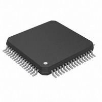
DS3106LN+ Maxim Integrated Products, DS3106LN+ Datasheet - Page 24

DS3106LN+
Manufacturer Part Number
DS3106LN+
Description
IC TIMING LINE CARD 64-LQFP
Manufacturer
Maxim Integrated Products
Type
Timing Card ICr
Datasheet
1.DS3106LN.pdf
(87 pages)
Specifications of DS3106LN+
Input
CMOS, LVDS, LVPECL, TTL
Output
CMOS, LVDS, LVPECL, TTL
Frequency - Max
312.5MHz
Voltage - Supply
1.62 V ~ 1.98 V
Operating Temperature
-40°C ~ 85°C
Mounting Type
Surface Mount
Package / Case
64-LQFP
Frequency-max
312.5MHz
Lead Free Status / RoHS Status
Lead free / RoHS Compliant
7.7.6 Frequency and Phase Measurement
Accurate measurement of frequency and phase can be accomplished using the T0 DPLL. The REFCLK signal
accuracy after being adjusted with MCLKFREQ is used for the frequency reference.
DPLL frequency measurements can be read from the FREQ field spanning registers FREQ1, FREQ2, and FREQ3.
This field indicates the frequency of the selected reference. This frequency measurement has a resolution of
0.0003068ppm over a 80ppm range. The value read from the FREQ field is the DPLL’s integral path value, which
is an averaged measurement with an averaging time inversely proportional to DPLL bandwidth.
DPLL phase measurements can be read from the PHASE field spanning registers
field indicates the phase difference seen by the phase detector. This phase measurement has a resolution of
approximately 0.703 degrees and is internally averaged with a -3dB attenuation point of approximately 100Hz.
Thus, for low DPLL bandwidths the PHASE field gives input phase wander in the frequency band from the DPLL
corner frequency up to 100Hz. This information could be used by software to compute a crude MTIE measurement.
7.7.7
The device is compliant with the jitter tolerance requirements of the standards listed in
360/180 PFD, jitter can be tolerated up to the point of eye closure. Either LOCK8K mode (see Section 7.4.2.2)
or the multicycle phase detector (see Section 7.7.4) should be used for high jitter tolerance.
7.7.8 Jitter Transfer
The transfer of jitter from the selected reference to the output clocks has a programmable transfer function that is
determined by the DPLL bandwidth. (See Section 7.7.2.) In the T0 DPLL, the 3dB corner frequency of the jitter
transfer function can be set to any of 7 positions from 18Hz to 400Hz.
7.7.9 Output Jitter and Wander
Several factors contribute to jitter and wander on the output clocks, including:
Jitter and wander amplitude on the selected reference (while in the locked state)
The jitter transfer characteristic of the device (while in the locked state)
The jitter and wander on the local oscillator clock signal (especially wander while in the holdover state)
The DPLL in the device has programmable bandwidth (see Section 7.7.2). With respect to jitter, the DPLL behaves
as a lowpass filter with a programmable pole. The bandwidth of the DPLL is low enough to strongly attenuate jitter
7.8
A total of four output clock pins, OC3, OC6, FSYNC, and MFSYNC, are available on the device. Output clocks OC3
and OC6 are individually configurable for a variety of frequencies. Output clocks FSYNC and MFSYNC are more
specialized, serving as an 8kHz frame sync (FSYNC) and a 2kHz multiframe sync (MFSYNC).
more detail on the capabilities of the output clock pins.
Table 7-5. Output Clock Capabilities
19-4629; Rev 4; 8/10
____________________________________________________________________________________________ DS3106
MFSYNC
OUTPUT
CLOCK
FSYNC
OC3
OC6
Output Clock Configuration
Input Jitter Tolerance
LVDS/LVPECL
CMOS/TTL
CMOS/TTL
FORMAT
SIGNAL
Frequency selection per Section
8kHz frame sync with programmable pulse width and polarity.
2kHz multiframe sync with programmable pulse width and polarity.
FREQUENCIES SUPPORTED
7.8.2.3
and
Table 7-6
PHASE1
Table
to
1-1. When using the
Table
and PHASE2. This
Table 7-5
7-12.
provides
24 of 87


