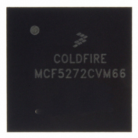
MCF5272CVM66 Freescale Semiconductor, MCF5272CVM66 Datasheet - Page 396

MCF5272CVM66
Manufacturer Part Number
MCF5272CVM66
Description
IC MPU 66MHZ COLDFIRE 196-MAPBGA
Manufacturer
Freescale Semiconductor
Series
MCF527xr
Specifications of MCF5272CVM66
Core Processor
Coldfire V2
Core Size
32-Bit
Speed
66MHz
Connectivity
EBI/EMI, Ethernet, I²C, SPI, UART/USART, USB
Peripherals
DMA, WDT
Number Of I /o
32
Program Memory Size
16KB (4K x 32)
Program Memory Type
ROM
Ram Size
1K x 32
Voltage - Supply (vcc/vdd)
3 V ~ 3.6 V
Oscillator Type
External
Operating Temperature
-40°C ~ 85°C
Package / Case
196-MAPBGA
Cpu Speed
66MHz
Embedded Interface Type
UART, QSPI, USB, TDM
Digital Ic Case Style
BGA
No. Of Pins
196
Supply Voltage Range
3V To 3.6V
Rohs Compliant
Yes
Family Name
MCF5xxx
Device Core
ColdFire
Device Core Size
32b
Frequency (max)
66MHz
Instruction Set Architecture
RISC
Supply Voltage 1 (typ)
3.3V
Operating Temp Range
-40C to 85C
Operating Temperature Classification
Industrial
Mounting
Surface Mount
Pin Count
196
Package Type
MA-BGA
Lead Free Status / RoHS Status
Lead free / RoHS Compliant
Eeprom Size
-
Data Converters
-
Lead Free Status / Rohs Status
Compliant
Available stocks
Company
Part Number
Manufacturer
Quantity
Price
Company:
Part Number:
MCF5272CVM66
Manufacturer:
MOT
Quantity:
3
Company:
Part Number:
MCF5272CVM66
Manufacturer:
Freescale Semiconductor
Quantity:
10 000
Part Number:
MCF5272CVM66
Manufacturer:
FREESCALE
Quantity:
20 000
Company:
Part Number:
MCF5272CVM66J
Manufacturer:
NSC
Quantity:
36
Company:
Part Number:
MCF5272CVM66J
Manufacturer:
Freescale Semiconductor
Quantity:
10 000
- Current page: 396 of 544
- Download datasheet (7Mb)
General Purpose I/O Module
17.2
The port control registers are used to configure all pins that carry signals multiplexed from different
on-chip modules. Each pin is configured with a two-bit field. Pin functions are referred to as
function 0b00–0b11. The function 0 signals corresponding to GPIO ports A and B are immediately
available after reset.
Wherever a signal function includes a GPIO port bit, the function defaults to an input after a reset and can
be read in the corresponding port data register.
Pin functions are generally grouped logically. For example, all UART1 signals are multiplexed with port
B and have the control register function code of 0b01.
There is no port C control register. Port C is enabled when the 16-bit-wide external data bus mode is
selected at reset by the input level on QSPI_DOUT/WSEL. The port D control register is used to configure
pins that have multiple functions (0b01 through 0b11) but no GPIO function.
17-2
0x0080
0x0084
0x0086
0x0088
0x008C
0x008E
0x0094
0x0096
0x0098
MBAR
Offset
Port Control Registers
Do not attempt to program a pin function that is not defined. Where no
function is defined, the function code is labeled ‘Reserved’ and is
considered invalid. Programming any control register field with a reserved
value has an unpredictable effect on the corresponding pin’s operation.
Reserved function codes cannot be reliably read. Attempts to read them
yield undetermined values.
Port C Data Direction Register (PCDDR)
Port B Data Direction Register (PBDDR)
Port A Data Direction Register (PADDR)
[31:24]
MCF5272 ColdFire
Reserved
Reserved
Reserved
Table 17-2. GPIO Port Register Memory Map
®
Integrated Microprocessor User’s Manual, Rev. 3
[23:16]
Port D Control Register (PDCNT)
Port B Control Register (PBCNT)
Port A Control Register (PACNT)
CAUTION
[15:8]
Port C Data Register (PCDAT)
Port B Data Register (PBDAT)
Port A Data Register (PADAT)
Reserved
Reserved
Reserved
Freescale Semiconductor
[7:0]
Related parts for MCF5272CVM66
Image
Part Number
Description
Manufacturer
Datasheet
Request
R
Part Number:
Description:
Mcf5272 Coldfire Integrated Microprocessor User
Manufacturer:
Freescale Semiconductor, Inc
Datasheet:

Part Number:
Description:
MCF5272 Interrupt Service Routine for the Physical Layer Interface Controller
Manufacturer:
Freescale Semiconductor / Motorola
Datasheet:
Part Number:
Description:
Manufacturer:
Freescale Semiconductor, Inc
Datasheet:
Part Number:
Description:
Manufacturer:
Freescale Semiconductor, Inc
Datasheet:
Part Number:
Description:
Manufacturer:
Freescale Semiconductor, Inc
Datasheet:
Part Number:
Description:
Manufacturer:
Freescale Semiconductor, Inc
Datasheet:
Part Number:
Description:
Manufacturer:
Freescale Semiconductor, Inc
Datasheet:
Part Number:
Description:
Manufacturer:
Freescale Semiconductor, Inc
Datasheet:
Part Number:
Description:
Manufacturer:
Freescale Semiconductor, Inc
Datasheet:
Part Number:
Description:
Manufacturer:
Freescale Semiconductor, Inc
Datasheet:
Part Number:
Description:
Manufacturer:
Freescale Semiconductor, Inc
Datasheet:
Part Number:
Description:
Manufacturer:
Freescale Semiconductor, Inc
Datasheet:
Part Number:
Description:
Manufacturer:
Freescale Semiconductor, Inc
Datasheet:
Part Number:
Description:
Manufacturer:
Freescale Semiconductor, Inc
Datasheet:
Part Number:
Description:
Manufacturer:
Freescale Semiconductor, Inc
Datasheet:


