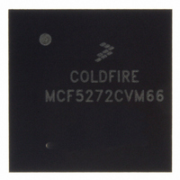
MCF5272CVM66 Freescale Semiconductor, MCF5272CVM66 Datasheet - Page 200

MCF5272CVM66
Manufacturer Part Number
MCF5272CVM66
Description
IC MPU 66MHZ COLDFIRE 196-MAPBGA
Manufacturer
Freescale Semiconductor
Series
MCF527xr
Specifications of MCF5272CVM66
Core Processor
Coldfire V2
Core Size
32-Bit
Speed
66MHz
Connectivity
EBI/EMI, Ethernet, I²C, SPI, UART/USART, USB
Peripherals
DMA, WDT
Number Of I /o
32
Program Memory Size
16KB (4K x 32)
Program Memory Type
ROM
Ram Size
1K x 32
Voltage - Supply (vcc/vdd)
3 V ~ 3.6 V
Oscillator Type
External
Operating Temperature
-40°C ~ 85°C
Package / Case
196-MAPBGA
Cpu Speed
66MHz
Embedded Interface Type
UART, QSPI, USB, TDM
Digital Ic Case Style
BGA
No. Of Pins
196
Supply Voltage Range
3V To 3.6V
Rohs Compliant
Yes
Family Name
MCF5xxx
Device Core
ColdFire
Device Core Size
32b
Frequency (max)
66MHz
Instruction Set Architecture
RISC
Supply Voltage 1 (typ)
3.3V
Operating Temp Range
-40C to 85C
Operating Temperature Classification
Industrial
Mounting
Surface Mount
Pin Count
196
Package Type
MA-BGA
Lead Free Status / RoHS Status
Lead free / RoHS Compliant
Eeprom Size
-
Data Converters
-
Lead Free Status / Rohs Status
Compliant
Available stocks
Company
Part Number
Manufacturer
Quantity
Price
Company:
Part Number:
MCF5272CVM66
Manufacturer:
MOT
Quantity:
3
Company:
Part Number:
MCF5272CVM66
Manufacturer:
Freescale Semiconductor
Quantity:
10 000
Part Number:
MCF5272CVM66
Manufacturer:
FREESCALE
Quantity:
20 000
Company:
Part Number:
MCF5272CVM66J
Manufacturer:
NSC
Quantity:
36
Company:
Part Number:
MCF5272CVM66J
Manufacturer:
Freescale Semiconductor
Quantity:
10 000
- Current page: 200 of 544
- Download datasheet (7Mb)
SDRAM Controller
To wake up the SDRAMs, SDCR[GSL] must be cleared. SDCR[SLEEP] remains set while the SDRAM
is exiting sleep mode and is cleared when the SDRAM completes the correct sequence to exit sleep mode.
9.8
The maximum performance of the SDRAM controller is determined by the required number of cycles for
page activation and precharge. The read access is influenced by the CAS latency. All SDRAM accesses
are in page mode. The following table shows the number of required cycles including all dead cycles for
each type of read/write SDRAM access. It assumes default timing configuration using an at least
PC100-compliant SDRAM device at 66 MHz. Page miss latency includes the cycles to precharge the last
open page and activate the new page before the read/write access. There are no precharge cycles when an
address hits an open page.
In
CLT = 1.
In
9-10
Table
Table
Single-beat read
Single-beat write
Burst read
Burst write
Table 9-9. SDRAM Controller Performance, 32-Bit Port, (RCD = 0, RP = 1) or (RCD = 1, RP = 0)
9-9, the timing configuration is RTP = 61, RC = negligible, RCD = 0 (or 1), RP = 1 (or 0), and
9-10, the timing configuration is RTP = 61, RC = negligible, RCD = 0, RP = 0, and CLT = 1.
Performance
Single-beat read
Single-beat write
Burst read
Burst write
Table 9-10. SDRAM Controller Performance, 32–Bit Port, (RCD = 0, RP = 0)
SDRAM Access
MCF5272 ColdFire
SDRAM Access
Page miss
Page hit
Page miss
Page hit
Page miss
Page hit
Page miss
Page hit
®
Page miss
Page hit
Page miss
Page hit
Page miss
Page hit
Page miss
Page hit
Integrated Microprocessor User’s Manual, Rev. 3
8
5
6
3
8-1-1-1 = 11
5-1-1-1 = 8
6-1-1-1 = 9
3-1-1-1 = 6
REG = 0, INV = 0
REG = 0, INV = 0
Number of System Clock Cycles
7-1-1-1 = 10
5-1-1-1 = 8
5-1-1-1 = 8
3-1-1-1 = 6
Number of System Clock Cycles
7
5
5
3
9
6
6
3
9-1-1-1 = 12
6-1-1-1 = 9
6-1-1-1 = 9
3-1-1-1 = 6
REG = 1, INV = 0
REG = 1, INV = 0
8-1-1-1 = 11
5-1-1-1 = 8
6-1-1-1 = 9
3-1-1-1 = 6
Freescale Semiconductor
8
6
5
3
Related parts for MCF5272CVM66
Image
Part Number
Description
Manufacturer
Datasheet
Request
R
Part Number:
Description:
Mcf5272 Coldfire Integrated Microprocessor User
Manufacturer:
Freescale Semiconductor, Inc
Datasheet:

Part Number:
Description:
MCF5272 Interrupt Service Routine for the Physical Layer Interface Controller
Manufacturer:
Freescale Semiconductor / Motorola
Datasheet:
Part Number:
Description:
Manufacturer:
Freescale Semiconductor, Inc
Datasheet:
Part Number:
Description:
Manufacturer:
Freescale Semiconductor, Inc
Datasheet:
Part Number:
Description:
Manufacturer:
Freescale Semiconductor, Inc
Datasheet:
Part Number:
Description:
Manufacturer:
Freescale Semiconductor, Inc
Datasheet:
Part Number:
Description:
Manufacturer:
Freescale Semiconductor, Inc
Datasheet:
Part Number:
Description:
Manufacturer:
Freescale Semiconductor, Inc
Datasheet:
Part Number:
Description:
Manufacturer:
Freescale Semiconductor, Inc
Datasheet:
Part Number:
Description:
Manufacturer:
Freescale Semiconductor, Inc
Datasheet:
Part Number:
Description:
Manufacturer:
Freescale Semiconductor, Inc
Datasheet:
Part Number:
Description:
Manufacturer:
Freescale Semiconductor, Inc
Datasheet:
Part Number:
Description:
Manufacturer:
Freescale Semiconductor, Inc
Datasheet:
Part Number:
Description:
Manufacturer:
Freescale Semiconductor, Inc
Datasheet:
Part Number:
Description:
Manufacturer:
Freescale Semiconductor, Inc
Datasheet:


