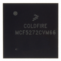
MCF5272CVM66 Freescale Semiconductor, MCF5272CVM66 Datasheet - Page 137

MCF5272CVM66
Manufacturer Part Number
MCF5272CVM66
Description
IC MPU 66MHZ COLDFIRE 196-MAPBGA
Manufacturer
Freescale Semiconductor
Series
MCF527xr
Specifications of MCF5272CVM66
Core Processor
Coldfire V2
Core Size
32-Bit
Speed
66MHz
Connectivity
EBI/EMI, Ethernet, I²C, SPI, UART/USART, USB
Peripherals
DMA, WDT
Number Of I /o
32
Program Memory Size
16KB (4K x 32)
Program Memory Type
ROM
Ram Size
1K x 32
Voltage - Supply (vcc/vdd)
3 V ~ 3.6 V
Oscillator Type
External
Operating Temperature
-40°C ~ 85°C
Package / Case
196-MAPBGA
Cpu Speed
66MHz
Embedded Interface Type
UART, QSPI, USB, TDM
Digital Ic Case Style
BGA
No. Of Pins
196
Supply Voltage Range
3V To 3.6V
Rohs Compliant
Yes
Family Name
MCF5xxx
Device Core
ColdFire
Device Core Size
32b
Frequency (max)
66MHz
Instruction Set Architecture
RISC
Supply Voltage 1 (typ)
3.3V
Operating Temp Range
-40C to 85C
Operating Temperature Classification
Industrial
Mounting
Surface Mount
Pin Count
196
Package Type
MA-BGA
Lead Free Status / RoHS Status
Lead free / RoHS Compliant
Eeprom Size
-
Data Converters
-
Lead Free Status / Rohs Status
Compliant
Available stocks
Company
Part Number
Manufacturer
Quantity
Price
Company:
Part Number:
MCF5272CVM66
Manufacturer:
MOT
Quantity:
3
Company:
Part Number:
MCF5272CVM66
Manufacturer:
Freescale Semiconductor
Quantity:
10 000
Part Number:
MCF5272CVM66
Manufacturer:
FREESCALE
Quantity:
20 000
Company:
Part Number:
MCF5272CVM66J
Manufacturer:
NSC
Quantity:
36
Company:
Part Number:
MCF5272CVM66J
Manufacturer:
Freescale Semiconductor
Quantity:
10 000
- Current page: 137 of 544
- Download datasheet (7Mb)
5.5.3
Table 5-17
each command. Issuing a BDM command when the processor is accessing debug module registers using
the WDEBUG instruction causes undefined behavior.
1
2
Unassigned command opcodes are reserved by Freescale. All unused command formats within any
revision level perform a
Freescale Semiconductor
Read A/D
register
Write A/D
register
Read memory
location
Write memory
location
Dump
memory block
Fill memory
block
Resume
execution
No operation
Read control
register
Write control
register
Read debug
module
register
Write debug
module
register
Command
General command effect and/or requirements on CPU operation:
- Halted. The CPU must be halted to perform this command.
- Steal. Command generates bus cycles that can be interleaved with bus accesses.
- Parallel. Command is executed in parallel with CPU activity.
0x4 is a three-bit field.
summarizes the BDM command set. Subsequent paragraphs contain detailed descriptions of
BDM Command Set
rareg/
rdreg
wareg/
wdreg
read
write
dump
fill
go
nop
rcreg
wcreg
rdmreg
wdmreg
Mnemonic
MCF5272 ColdFire
NOP
Read the selected address or data register and return
the results through the serial interface.
Write the data operand to the specified address or data
register.
Read the data at the memory location specified by the
longword address.
Write the operand data to the memory location
specified by the longword address.
Used with
initial
the block and to retrieve the first result. A
command retrieves subsequent operands.
Used with
WRITE
block and to supply the first operand. A
writes subsequent operands.
The pipeline is flushed and refilled before resuming
instruction execution at the current PC.
Perform no operation; may be used as a null command.
Read the system control register.
Write the operand data to the system control register.
Read the debug module register.
Write the operand data to the debug module register.
and return the illegal command response.
READ
is executed to set up the starting address of the
WRITE
READ
Table 5-17. BDM Command Summary
is executed to set up the starting address of
to dump large blocks of memory. An
®
to fill large blocks of memory. An initial
Integrated Microprocessor User’s Manual, Rev. 3
Description
FILL
DUMP
command
Parallel
Parallel
Parallel
State
Halted
Halted
Halted
Halted
Halted
Steal
Steal
Steal
Steal
CPU
1
5.5.3.3.10 0x2880
5.5.3.3.11 0x2D {0x4
5.5.3.3.12 0x2C {0x4
5.5.3.3.1
5.5.3.3.2
5.5.3.3.3
5.5.3.3.4
5.5.3.3.5
5.5.3.3.6
5.5.3.3.7
5.5.3.3.8
5.5.3.3.9
Section
0x218 {A/D,
Reg[2:0]}
0x208 {A/D,
Reg[2:0]}
0x1900—byte
0x1940—word
0x1980—lword
0x1800—byte
0x1840—word
0x1880—lword
0x1D00—byte
0x1D40—word
0x1D80—lword
0x1C00—byte
0x1C40—word
0x1C80—lword
0x0C00
0x0000
0x2980
DRc[4:0]}
DRc[4:0]}
Debug Support
Command
(Hex)
2
2
5-19
Related parts for MCF5272CVM66
Image
Part Number
Description
Manufacturer
Datasheet
Request
R
Part Number:
Description:
Mcf5272 Coldfire Integrated Microprocessor User
Manufacturer:
Freescale Semiconductor, Inc
Datasheet:

Part Number:
Description:
MCF5272 Interrupt Service Routine for the Physical Layer Interface Controller
Manufacturer:
Freescale Semiconductor / Motorola
Datasheet:
Part Number:
Description:
Manufacturer:
Freescale Semiconductor, Inc
Datasheet:
Part Number:
Description:
Manufacturer:
Freescale Semiconductor, Inc
Datasheet:
Part Number:
Description:
Manufacturer:
Freescale Semiconductor, Inc
Datasheet:
Part Number:
Description:
Manufacturer:
Freescale Semiconductor, Inc
Datasheet:
Part Number:
Description:
Manufacturer:
Freescale Semiconductor, Inc
Datasheet:
Part Number:
Description:
Manufacturer:
Freescale Semiconductor, Inc
Datasheet:
Part Number:
Description:
Manufacturer:
Freescale Semiconductor, Inc
Datasheet:
Part Number:
Description:
Manufacturer:
Freescale Semiconductor, Inc
Datasheet:
Part Number:
Description:
Manufacturer:
Freescale Semiconductor, Inc
Datasheet:
Part Number:
Description:
Manufacturer:
Freescale Semiconductor, Inc
Datasheet:
Part Number:
Description:
Manufacturer:
Freescale Semiconductor, Inc
Datasheet:
Part Number:
Description:
Manufacturer:
Freescale Semiconductor, Inc
Datasheet:
Part Number:
Description:
Manufacturer:
Freescale Semiconductor, Inc
Datasheet:


