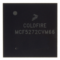
MCF5272CVM66 Freescale Semiconductor, MCF5272CVM66 Datasheet - Page 193

MCF5272CVM66
Manufacturer Part Number
MCF5272CVM66
Description
IC MPU 66MHZ COLDFIRE 196-MAPBGA
Manufacturer
Freescale Semiconductor
Series
MCF527xr
Specifications of MCF5272CVM66
Core Processor
Coldfire V2
Core Size
32-Bit
Speed
66MHz
Connectivity
EBI/EMI, Ethernet, I²C, SPI, UART/USART, USB
Peripherals
DMA, WDT
Number Of I /o
32
Program Memory Size
16KB (4K x 32)
Program Memory Type
ROM
Ram Size
1K x 32
Voltage - Supply (vcc/vdd)
3 V ~ 3.6 V
Oscillator Type
External
Operating Temperature
-40°C ~ 85°C
Package / Case
196-MAPBGA
Cpu Speed
66MHz
Embedded Interface Type
UART, QSPI, USB, TDM
Digital Ic Case Style
BGA
No. Of Pins
196
Supply Voltage Range
3V To 3.6V
Rohs Compliant
Yes
Family Name
MCF5xxx
Device Core
ColdFire
Device Core Size
32b
Frequency (max)
66MHz
Instruction Set Architecture
RISC
Supply Voltage 1 (typ)
3.3V
Operating Temp Range
-40C to 85C
Operating Temperature Classification
Industrial
Mounting
Surface Mount
Pin Count
196
Package Type
MA-BGA
Lead Free Status / RoHS Status
Lead free / RoHS Compliant
Eeprom Size
-
Data Converters
-
Lead Free Status / Rohs Status
Compliant
Available stocks
Company
Part Number
Manufacturer
Quantity
Price
Company:
Part Number:
MCF5272CVM66
Manufacturer:
MOT
Quantity:
3
Company:
Part Number:
MCF5272CVM66
Manufacturer:
Freescale Semiconductor
Quantity:
10 000
Part Number:
MCF5272CVM66
Manufacturer:
FREESCALE
Quantity:
20 000
Company:
Part Number:
MCF5272CVM66J
Manufacturer:
NSC
Quantity:
36
Company:
Part Number:
MCF5272CVM66J
Manufacturer:
Freescale Semiconductor
Quantity:
10 000
- Current page: 193 of 544
- Download datasheet (7Mb)
Figure 9-2
can vary from 16–256 Mbits.
Freescale Semiconductor
SDRAMCS/CS7
SDCLKE
SDCLK
Signal
SDWE
DQML
GND
GND
VDD
VDD
VDD
VDD
VDD
DQ0
DQ1
DQ2
DQ3
DQ4
DQ5
DQ6
DQ7
CAS
RAS
R/W
BA0
BA1
A10
is the pinout of a 16-bit SDRAM in a 54-pin TSOP (thin, small-outline package) package. Size
CS
A0
A1
A2
A3
DQML
GND
GND
VDD
VDD
VDD
VDD
VDD
DQ0
DQ1
DQ2
DQ3
DQ4
DQ5
DQ6
DQ7
CAS
RAS
R/W
BA0
BA1
A10
CS
SDRAM (bus) clock (same frequency as CPU clock). This dedicated output reduces setup and hold
time uncertainty due to process and temperature variations. SDCLK is disabled for SDRAM
power-down mode.
SDRAM clock enable
SDRAM chip select/CS7. The SDRAM is assigned to CS7 (SDRAMCS) of the device chip select
module.
SDRAM write enable
A0
A1
A2
A3
MCF5272 ColdFire
Table 9-1. SDRAM Controller Signal Descriptions (continued)
DQML
GND
GND
VDD
VDD
VDD
VDD
VDD
DQ0
DQ1
DQ2
DQ3
DQ4
DQ5
DQ6
DQ7
CAS
RAS
R/W
BA0
BA1
A10
Figure 9-2. 54-Pin TSOP SDRAM Pin Definition
CS
A0
A1
A2
A3
1
2
3
4
5
6
7
8
9
10
11
12
13
14
15
16
17
18
19
20
21
22
23
24
25
26
27
®
Integrated Microprocessor User’s Manual, Rev. 3
128 Mbit
256 Mbit
64 Mbit
Description
54
53
52
51
50
49
48
47
46
45
44
43
42
41
40
39
38
37
36
35
34
33
32
31
30
29
28
GND
DQ15
GND
DQ14
DQ13
VDD
DQ12
DQ11
GND
DQ10
DQ9
VDD
DQ8
GND
NC
DQMH
CLK
CKE
A12
A11
A9
A8
A7
A6
A5
A4
GND
GND
DQ15
GND
DQ14
DQ13
VDD
DQ12
DQ11
GND
DQ10
DQ9
VDD
DQ8
GND
NC
DQMH
CLK
CKE
A12
A11
A9
A8
A7
A6
A5
A4
GND
GND
DQ15
GND
DQ14
DQ13
VDD
DQ12
DQ11
GND
DQ10
DQ9
VDD
DQ8
GND
NC
DQMH
CLK
CKE
A12
A11
A9
A8
A7
A6
A5
A4
GND
SDRAM Controller
9-3
Related parts for MCF5272CVM66
Image
Part Number
Description
Manufacturer
Datasheet
Request
R
Part Number:
Description:
Mcf5272 Coldfire Integrated Microprocessor User
Manufacturer:
Freescale Semiconductor, Inc
Datasheet:

Part Number:
Description:
MCF5272 Interrupt Service Routine for the Physical Layer Interface Controller
Manufacturer:
Freescale Semiconductor / Motorola
Datasheet:
Part Number:
Description:
Manufacturer:
Freescale Semiconductor, Inc
Datasheet:
Part Number:
Description:
Manufacturer:
Freescale Semiconductor, Inc
Datasheet:
Part Number:
Description:
Manufacturer:
Freescale Semiconductor, Inc
Datasheet:
Part Number:
Description:
Manufacturer:
Freescale Semiconductor, Inc
Datasheet:
Part Number:
Description:
Manufacturer:
Freescale Semiconductor, Inc
Datasheet:
Part Number:
Description:
Manufacturer:
Freescale Semiconductor, Inc
Datasheet:
Part Number:
Description:
Manufacturer:
Freescale Semiconductor, Inc
Datasheet:
Part Number:
Description:
Manufacturer:
Freescale Semiconductor, Inc
Datasheet:
Part Number:
Description:
Manufacturer:
Freescale Semiconductor, Inc
Datasheet:
Part Number:
Description:
Manufacturer:
Freescale Semiconductor, Inc
Datasheet:
Part Number:
Description:
Manufacturer:
Freescale Semiconductor, Inc
Datasheet:
Part Number:
Description:
Manufacturer:
Freescale Semiconductor, Inc
Datasheet:
Part Number:
Description:
Manufacturer:
Freescale Semiconductor, Inc
Datasheet:


