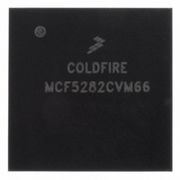
MCF5282CVM66 Freescale Semiconductor, MCF5282CVM66 Datasheet - Page 527

MCF5282CVM66
Manufacturer Part Number
MCF5282CVM66
Description
IC MPU 512K 66MHZ 256-MAPBGA
Manufacturer
Freescale Semiconductor
Series
MCF528xr
Datasheet
1.MCF5216CVM66J.pdf
(766 pages)
Specifications of MCF5282CVM66
Core Processor
Coldfire V2
Core Size
32-Bit
Speed
66MHz
Connectivity
CAN, EBI/EMI, Ethernet, I²C, SPI, UART/USART
Peripherals
DMA, LVD, POR, PWM, WDT
Number Of I /o
150
Program Memory Size
512KB (512K x 8)
Program Memory Type
FLASH
Ram Size
64K x 8
Voltage - Supply (vcc/vdd)
2.7 V ~ 3.6 V
Data Converters
A/D 8x10b
Oscillator Type
External
Operating Temperature
-40°C ~ 85°C
Package / Case
256-MAPBGA
Controller Family/series
ColdFire
No. Of I/o's
150
Ram Memory Size
64KB
Cpu Speed
66.67MHz
Embedded Interface Type
CAN, I2C, SPI, UART
No. Of Pwm Channels
8
Rohs Compliant
Yes
Lead Free Status / RoHS Status
Lead free / RoHS Compliant
Eeprom Size
-
Available stocks
Company
Part Number
Manufacturer
Quantity
Price
Company:
Part Number:
MCF5282CVM66
Manufacturer:
FREESCAL
Quantity:
152
Company:
Part Number:
MCF5282CVM66
Manufacturer:
Freescale Semiconductor
Quantity:
10 000
Part Number:
MCF5282CVM66
Manufacturer:
NXP/恩智浦
Quantity:
20 000
Company:
Part Number:
MCF5282CVM66J
Manufacturer:
Freescale Semiconductor
Quantity:
10 000
- Current page: 527 of 766
- Download datasheet (9Mb)
26.4
26.4.1
The initial pin function is determined during reset configuration. The pin assignment registers allow the
user to select between digital I/O or another pin function after reset.
In single-chip mode, all pins are configured as digital I/O by default, except for debug data pins
(DDATA[3:0]) and processor status pins (PST[3:0]). These pins are configured for their primary functions
by default in all modes.
Every digital I/O pin is individually configurable as an input or an output via a data direction register
(DDRn).
Every port has an output data register (PORTn) and a pin data register (PORTnP/SETn) to monitor and
control the state of its pins. Data written to a PORTn register is stored and then driven to the corresponding
port n pins configured as outputs.
Reading a PORTn register returns the current state of the register regardless of the state of the
corresponding pins.
Reading a PORTnP/PSETn register returns the current state of the corresponding pins when configured as
digital I/O, regardless of whether the pins are inputs or outputs.
Every port has a PORTnP/SETn register and a clear register (CLRn) for setting or clearing individual bits
in the PORTn register.
In master mode, port A and B function as the upper external data bus, D[31:16]. When the PCDPA bit is
set, ports C and D function as the lower external data bus, D[15:0]. Ports E–J are configured to support
external memory functions.
The ports module does not generate interrupt requests.
26.4.2
Input data on all pins configured as digital I/O is synchronized to the rising edge of CLKOUT, as shown
in
Freescale Semiconductor
Figure
Bits
2
1
0
26-30.
Functional Description
Overview
Port Digital I/O Timing
PUAPA2
PUAPA1
PUAPA0
Name
MCF5282 and MCF5216 ColdFire Microcontroller User’s Manual, Rev. 3
Port UA pin assignment 2. This bit configures the port UA2 pin for its primary function
(UTXD1) or digital I/O.
1 Port UA2 pin configured for primary function (UTXD1)
0 Port UA2 pin configured for digital I/O
Port UA pin assignment 1. This bit configures the port UA1 pin for its primary function
(URXD0) or digital I/O.
1 Port UA1 pin configured for primary function (URXD0)
0 Port UA1 pin configured for digital I/O
Port UA pin assignment 0. This bit configures the port UA0 pin for its primary function
(UTXD0) or digital I/O.
1 Port UA0 pin configured for primary function (UTXD0)
0 Port UA0 pin configured for digital I/O
Table 26-19. PUAPAR Field Descriptions (continued)
Description
General Purpose I/O Module
26-27
Related parts for MCF5282CVM66
Image
Part Number
Description
Manufacturer
Datasheet
Request
R
Part Number:
Description:
Mcf5282 And Mcf5216 Coldfire Microcontroller User�s Manual
Manufacturer:
Freescale Semiconductor, Inc
Datasheet:
Part Number:
Description:
Manufacturer:
Freescale Semiconductor, Inc
Datasheet:
Part Number:
Description:
Manufacturer:
Freescale Semiconductor, Inc
Datasheet:
Part Number:
Description:
Manufacturer:
Freescale Semiconductor, Inc
Datasheet:
Part Number:
Description:
Manufacturer:
Freescale Semiconductor, Inc
Datasheet:
Part Number:
Description:
Manufacturer:
Freescale Semiconductor, Inc
Datasheet:
Part Number:
Description:
Manufacturer:
Freescale Semiconductor, Inc
Datasheet:
Part Number:
Description:
Manufacturer:
Freescale Semiconductor, Inc
Datasheet:
Part Number:
Description:
Manufacturer:
Freescale Semiconductor, Inc
Datasheet:
Part Number:
Description:
Manufacturer:
Freescale Semiconductor, Inc
Datasheet:
Part Number:
Description:
Manufacturer:
Freescale Semiconductor, Inc
Datasheet:
Part Number:
Description:
Manufacturer:
Freescale Semiconductor, Inc
Datasheet:
Part Number:
Description:
Manufacturer:
Freescale Semiconductor, Inc
Datasheet:
Part Number:
Description:
Manufacturer:
Freescale Semiconductor, Inc
Datasheet:
Part Number:
Description:
Manufacturer:
Freescale Semiconductor, Inc
Datasheet:


