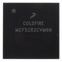
MCF5282CVM66 Freescale Semiconductor, MCF5282CVM66 Datasheet - Page 276

MCF5282CVM66
Manufacturer Part Number
MCF5282CVM66
Description
IC MPU 512K 66MHZ 256-MAPBGA
Manufacturer
Freescale Semiconductor
Series
MCF528xr
Datasheet
1.MCF5216CVM66J.pdf
(766 pages)
Specifications of MCF5282CVM66
Core Processor
Coldfire V2
Core Size
32-Bit
Speed
66MHz
Connectivity
CAN, EBI/EMI, Ethernet, I²C, SPI, UART/USART
Peripherals
DMA, LVD, POR, PWM, WDT
Number Of I /o
150
Program Memory Size
512KB (512K x 8)
Program Memory Type
FLASH
Ram Size
64K x 8
Voltage - Supply (vcc/vdd)
2.7 V ~ 3.6 V
Data Converters
A/D 8x10b
Oscillator Type
External
Operating Temperature
-40°C ~ 85°C
Package / Case
256-MAPBGA
Controller Family/series
ColdFire
No. Of I/o's
150
Ram Memory Size
64KB
Cpu Speed
66.67MHz
Embedded Interface Type
CAN, I2C, SPI, UART
No. Of Pwm Channels
8
Rohs Compliant
Yes
Lead Free Status / RoHS Status
Lead free / RoHS Compliant
Eeprom Size
-
Available stocks
Company
Part Number
Manufacturer
Quantity
Price
Company:
Part Number:
MCF5282CVM66
Manufacturer:
FREESCAL
Quantity:
152
Company:
Part Number:
MCF5282CVM66
Manufacturer:
Freescale Semiconductor
Quantity:
10 000
Part Number:
MCF5282CVM66
Manufacturer:
NXP/恩智浦
Quantity:
20 000
Company:
Part Number:
MCF5282CVM66J
Manufacturer:
Freescale Semiconductor
Quantity:
10 000
- Current page: 276 of 766
- Download datasheet (9Mb)
Synchronous DRAM Controller Module
15.2.1
Table 15-2
15.2.2
The DRAM controller registers memory map is shown in
15.2.2.1 DRAM Control Register (DCR)
The DCR, shown in
15-4
SRAS
SCAS
DRAMW
SDRAM_CS[1:0
]
SCKE
BS[3:0]
IPSBAR
Signal
Offset
0x04C
0x040
0x044
0x048
0x050
0x054
DRAM Controller Signals
describes the behavior of DRAM signals in synchronous mode.
Memory Map for SDRAMC Registers
Synchronous row address strobe. Indicates a valid SDRAM row address is present and can be latched by
the SDRAM. SRAS should be connected to the corresponding SDRAM SRAS.
Synchronous column address strobe. Indicates a valid column address is present and can be latched by
the SDRAM. SCAS should be connected to the corresponding SDRAM SCAS.
DRAM read/write. Asserted for write operations and negated for read operations.
Row address strobe. Select each memory block of SDRAMs connected to the processor. One
SDRAM_CS signal selects one SDRAM block and connects to the corresponding CS signals.
Synchronous DRAM clock enable. Connected directly to the CKE (clock enable) signal of SDRAMs.
Enables and disables the clock internal to SDRAM. When CKE is low, memory can enter a power-down
mode in which operations are suspended or capable of entering self-refresh mode. SCKE functionality is
controlled by DCR[COC]. For designs using external multiplexing, setting COC allows SCKE to provide
command-bit functionality.
Column address strobe. BS[3:0] function as byte enables to the SDRAMs. They connect to the BS signals
(or mask qualifiers) of the SDRAMs.
DRAM control register (DCR) [p. 15-4]
Figure
[31:24]
MCF5282 and MCF5216 ColdFire Microcontroller User’s Manual, Rev. 3
Table 15-2. Synchronous DRAM Signal Connections
15-2, controls refresh logic.
Table 15-3. DRAM Controller Registers
DRAM address and control register 0 (DACR0) [p. 15-6]
DRAM address and control register 1 (DACR1) [p. 15-6]
DRAM mask register block 0 (DMR0) [p. 15-8]
DRAM mask register block 1 (DMR1) [p. 15-8]
[23:16]
Description
—
Table
15-3.
[15:8]
—
Freescale Semiconductor
[7:0]
Related parts for MCF5282CVM66
Image
Part Number
Description
Manufacturer
Datasheet
Request
R
Part Number:
Description:
Mcf5282 And Mcf5216 Coldfire Microcontroller User�s Manual
Manufacturer:
Freescale Semiconductor, Inc
Datasheet:
Part Number:
Description:
Manufacturer:
Freescale Semiconductor, Inc
Datasheet:
Part Number:
Description:
Manufacturer:
Freescale Semiconductor, Inc
Datasheet:
Part Number:
Description:
Manufacturer:
Freescale Semiconductor, Inc
Datasheet:
Part Number:
Description:
Manufacturer:
Freescale Semiconductor, Inc
Datasheet:
Part Number:
Description:
Manufacturer:
Freescale Semiconductor, Inc
Datasheet:
Part Number:
Description:
Manufacturer:
Freescale Semiconductor, Inc
Datasheet:
Part Number:
Description:
Manufacturer:
Freescale Semiconductor, Inc
Datasheet:
Part Number:
Description:
Manufacturer:
Freescale Semiconductor, Inc
Datasheet:
Part Number:
Description:
Manufacturer:
Freescale Semiconductor, Inc
Datasheet:
Part Number:
Description:
Manufacturer:
Freescale Semiconductor, Inc
Datasheet:
Part Number:
Description:
Manufacturer:
Freescale Semiconductor, Inc
Datasheet:
Part Number:
Description:
Manufacturer:
Freescale Semiconductor, Inc
Datasheet:
Part Number:
Description:
Manufacturer:
Freescale Semiconductor, Inc
Datasheet:
Part Number:
Description:
Manufacturer:
Freescale Semiconductor, Inc
Datasheet:


