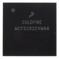
MCF5282CVM66 Freescale Semiconductor, MCF5282CVM66 Datasheet - Page 270

MCF5282CVM66
Manufacturer Part Number
MCF5282CVM66
Description
IC MPU 512K 66MHZ 256-MAPBGA
Manufacturer
Freescale Semiconductor
Series
MCF528xr
Datasheet
1.MCF5216CVM66J.pdf
(766 pages)
Specifications of MCF5282CVM66
Core Processor
Coldfire V2
Core Size
32-Bit
Speed
66MHz
Connectivity
CAN, EBI/EMI, Ethernet, I²C, SPI, UART/USART
Peripherals
DMA, LVD, POR, PWM, WDT
Number Of I /o
150
Program Memory Size
512KB (512K x 8)
Program Memory Type
FLASH
Ram Size
64K x 8
Voltage - Supply (vcc/vdd)
2.7 V ~ 3.6 V
Data Converters
A/D 8x10b
Oscillator Type
External
Operating Temperature
-40°C ~ 85°C
Package / Case
256-MAPBGA
Controller Family/series
ColdFire
No. Of I/o's
150
Ram Memory Size
64KB
Cpu Speed
66.67MHz
Embedded Interface Type
CAN, I2C, SPI, UART
No. Of Pwm Channels
8
Rohs Compliant
Yes
Lead Free Status / RoHS Status
Lead free / RoHS Compliant
Eeprom Size
-
Available stocks
Company
Part Number
Manufacturer
Quantity
Price
Company:
Part Number:
MCF5282CVM66
Manufacturer:
FREESCAL
Quantity:
152
Company:
Part Number:
MCF5282CVM66
Manufacturer:
Freescale Semiconductor
Quantity:
10 000
Part Number:
MCF5282CVM66
Manufacturer:
NXP/恩智浦
Quantity:
20 000
Company:
Part Number:
MCF5282CVM66J
Manufacturer:
Freescale Semiconductor
Quantity:
10 000
- Current page: 270 of 766
- Download datasheet (9Mb)
Signal Descriptions
14.2.14.2 Development Serial Clock/Test Reset (DSCLK/TRST)
Debug mode operation: DSCLK is selected. DSCLK is the development serial clock for the serial interface
to the debug module. The maximum DSCLK frequency is 1/5 CLKIN.
JTAG mode operation: TRST is selected. TRST asynchronously resets the internal JTAG controller to the
test logic reset state, causing the JTAG instruction register to choose the bypass instruction. When this
occurs, JTAG logic is benign and does not interfere with normal device functionality.
Although TRST is asynchronous, Freescale recommends that it makes an asserted-to-negated transition
only while TMS is held high. TRST has an internal pull-up resistor so if it is not driven low, it defaults to
a logic level of 1. If TRST is not used, it can be tied to ground or, if TCK is clocked, to V
to ground places the JTAG controller in test logic reset state immediately. Tying it to V
controller (if TMS is a logic level of 1) to eventually enter test logic reset state after 5 TCK clocks.
14.2.14.3 Breakpoint/Test Mode Select (BKPT/TMS)
Debug mode operation: If JTAG_EN is low, BKPT is selected. BKPT signals a hardware breakpoint to the
processor in debug mode.
JTAG mode operation: TMS is selected. The TMS input provides information to determine the JTAG test
operation mode. The state of TMS and the internal 16-state JTAG controller state machine at the rising
edge of TCK determine whether the JTAG controller holds its current state or advances to the next state.
This directly controls whether JTAG data or instruction operations occur. TMS has an internal pull-up
resistor so that if it is not driven low, it defaults to a logic level of 1. But if TMS is not used, it should be
tied to V
14.2.14.4 Development Serial Input/Test Data (DSI/TDI)
Debug mode operation: If JTAG_EN is low, DSI is selected. DSI provides the single-bit communication
for debug module commands.
JTAG mode operation: TDI is selected. TDI provides the serial data port for loading the various JTAG
boundary scan, bypass, and instruction registers. Shifting in data depends on the state of the JTAG
controller state machine and the instruction in the instruction register. Shifts occur on the TCK rising edge.
TDI has an internal pull-up resistor, so when not driven low it defaults to high. But if TDI is not used, it
should be tied to V
14.2.14.5 Development Serial Output/Test Data (DSO/TDO)
Debug mode operation: DSO is selected. DSO provides single-bit communication for debug module
responses.
JTAG mode operation: TDO is selected. The TDO output provides the serial data port for outputting data
from JTAG logic. Shifting out data depends on the JTAG controller state machine and the instruction in
the instruction register. Data shifting occurs on the falling edge of TCK. When TDO is not outputting test
data, it is three-stated. TDO can be three-stated to allow bused or parallel connections to other devices
having JTAG.
14.2.14.6 Test Clock (TCLK)
TCK is the dedicated JTAG test logic clock independent of the processor clock. Various JTAG operations
occur on the rising or falling edge of TCK. Holding TCK high or low for an indefinite period does not
cause JTAG test logic to lose state information. If TCK is not used, it must be tied to ground.
14-30
DD
.
DD
.
MCF5282 and MCF5216 ColdFire Microcontroller User’s Manual, Rev. 3
Freescale Semiconductor
DD
DD
causes the JTAG
. Tying TRST
Related parts for MCF5282CVM66
Image
Part Number
Description
Manufacturer
Datasheet
Request
R
Part Number:
Description:
Mcf5282 And Mcf5216 Coldfire Microcontroller User�s Manual
Manufacturer:
Freescale Semiconductor, Inc
Datasheet:
Part Number:
Description:
Manufacturer:
Freescale Semiconductor, Inc
Datasheet:
Part Number:
Description:
Manufacturer:
Freescale Semiconductor, Inc
Datasheet:
Part Number:
Description:
Manufacturer:
Freescale Semiconductor, Inc
Datasheet:
Part Number:
Description:
Manufacturer:
Freescale Semiconductor, Inc
Datasheet:
Part Number:
Description:
Manufacturer:
Freescale Semiconductor, Inc
Datasheet:
Part Number:
Description:
Manufacturer:
Freescale Semiconductor, Inc
Datasheet:
Part Number:
Description:
Manufacturer:
Freescale Semiconductor, Inc
Datasheet:
Part Number:
Description:
Manufacturer:
Freescale Semiconductor, Inc
Datasheet:
Part Number:
Description:
Manufacturer:
Freescale Semiconductor, Inc
Datasheet:
Part Number:
Description:
Manufacturer:
Freescale Semiconductor, Inc
Datasheet:
Part Number:
Description:
Manufacturer:
Freescale Semiconductor, Inc
Datasheet:
Part Number:
Description:
Manufacturer:
Freescale Semiconductor, Inc
Datasheet:
Part Number:
Description:
Manufacturer:
Freescale Semiconductor, Inc
Datasheet:
Part Number:
Description:
Manufacturer:
Freescale Semiconductor, Inc
Datasheet:


