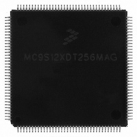
MC9S12XDT256MAG Freescale Semiconductor, MC9S12XDT256MAG Datasheet - Page 677

MC9S12XDT256MAG
Manufacturer Part Number
MC9S12XDT256MAG
Description
IC MCU 256K FLASH 144-LQFP
Manufacturer
Freescale Semiconductor
Series
HCS12r
Datasheet
1.MC9S12XD64CAA.pdf
(1348 pages)
Specifications of MC9S12XDT256MAG
Core Processor
HCS12X
Core Size
16-Bit
Speed
80MHz
Connectivity
CAN, EBI/EMI, I²C, IrDA, LIN, SCI, SPI
Peripherals
LVD, POR, PWM, WDT
Number Of I /o
119
Program Memory Size
256KB (256K x 8)
Program Memory Type
FLASH
Eeprom Size
4K x 8
Ram Size
16K x 8
Voltage - Supply (vcc/vdd)
2.35 V ~ 5.5 V
Data Converters
A/D 24x10b
Oscillator Type
External
Operating Temperature
-40°C ~ 125°C
Package / Case
144-LQFP
Processor Series
S12XD
Core
HCS12
Data Bus Width
16 bit
Data Ram Size
16 KB
Interface Type
CAN/I2C/SCI/SPI
Maximum Clock Frequency
40 MHz
Number Of Programmable I/os
119
Number Of Timers
12
Operating Supply Voltage
0 V to 5.5 V
Maximum Operating Temperature
+ 125 C
Mounting Style
SMD/SMT
3rd Party Development Tools
EWHCS12
Development Tools By Supplier
EVB9S12XDP512E
Minimum Operating Temperature
- 40 C
On-chip Adc
2 (24-ch x 10-bit)
Lead Free Status / RoHS Status
Lead free / RoHS Compliant
Available stocks
Company
Part Number
Manufacturer
Quantity
Price
Company:
Part Number:
MC9S12XDT256MAG
Manufacturer:
Freescale Semiconductor
Quantity:
10 000
- Current page: 677 of 1348
- Download datasheet (8Mb)
18.4.2.3
The global memory spaces reserved for the internal resources (RAM, EEPROM, and FLASH) are not
determined by the MMC module. Size of the individual internal resources are however fixed in the design
of the device cannot be changed by the user. Please refer to the Device User Guide for further details.
Figure 18-23
the memory spaces have fixed top addresses.
When the device is operating in expanded modes except emulation single-chip mode, accesses to global
addresses which are not occupied by the on-chip resources (unimplemented areas or external memory
space) result in accesses to the external bus (see
In emulation single-chip mode, accesses to global addresses which are not occupied by the on-chip
resources (unimplemented areas) result in accesses to the external bus. CPU accesses to global addresses
which are occupied by external memory space result in an illegal access reset (system reset). BDM
accesses to the external space are performed but the data will be undefined.
In single-chip modes accesses by the CPU (except for firmware commands) to any of the unimplemented
areas (see
unimplemented areas are allowed but the data will be undefined.
No misaligned word access from the BDM module will occur; these accesses are blocked in the BDM
module (Refer to BDM Block Guide).
Misaligned word access to the last location of RAM is performed but the data will be undefined.
Misaligned word access to the last location of any global page (64 Kbyte) by any global instruction, is
performed by accessing the last byte of the page and the first byte of the same page, considering the above
mentioned misaligned access cases.
The non-internal resources (unimplemented areas or external space) are used to generate the chip selects
(CS0,CS1,CS2 and CS3) (see
expanded and special test modes (see
Freescale Semiconductor
Figure
and
Implemented Memory Map
1
2
Table 18-20
18-23) will result in an illegal access reset (system reset). BDM accesses to the
RAMSIZE is the hexadecimal value of RAM SIZE in bytes
EEPROMSIZE is the hexadecimal value of EEPROM SIZE in bytes
Internal Resource
EEPROM
RAM
Table 18-20. Global Implemented Memory Space
show the memory spaces occupied by the on-chip resources. Please note that
Figure
MC9S12XDP512 Data Sheet, Rev. 2.21
18-23), which are only active in normal expanded, emulation
Section 18.3.2.1, “MMC Control Register
EEPROM_LOW = 0x14_0000 minus EEPROMSIZE
RAM_LOW = 0x10_0000 minus RAMSIZE
Figure
18-23).
$Address
Chapter 18 Memory Mapping Control (S12XMMCV3)
(MMCCTL0)).
1
2
677
Related parts for MC9S12XDT256MAG
Image
Part Number
Description
Manufacturer
Datasheet
Request
R

Part Number:
Description:
16-BIT MICROPROCESSOR FAMILY
Manufacturer:
FREESCALE [Freescale Semiconductor, Inc]
Datasheet:
Part Number:
Description:
Manufacturer:
Freescale Semiconductor, Inc
Datasheet:
Part Number:
Description:
Manufacturer:
Freescale Semiconductor, Inc
Datasheet:
Part Number:
Description:
Manufacturer:
Freescale Semiconductor, Inc
Datasheet:
Part Number:
Description:
Manufacturer:
Freescale Semiconductor, Inc
Datasheet:
Part Number:
Description:
Manufacturer:
Freescale Semiconductor, Inc
Datasheet:
Part Number:
Description:
Manufacturer:
Freescale Semiconductor, Inc
Datasheet:
Part Number:
Description:
Manufacturer:
Freescale Semiconductor, Inc
Datasheet:
Part Number:
Description:
Manufacturer:
Freescale Semiconductor, Inc
Datasheet:
Part Number:
Description:
Manufacturer:
Freescale Semiconductor, Inc
Datasheet:
Part Number:
Description:
Manufacturer:
Freescale Semiconductor, Inc
Datasheet:
Part Number:
Description:
Manufacturer:
Freescale Semiconductor, Inc
Datasheet:
Part Number:
Description:
Manufacturer:
Freescale Semiconductor, Inc
Datasheet:
Part Number:
Description:
Manufacturer:
Freescale Semiconductor, Inc
Datasheet:
Part Number:
Description:
Manufacturer:
Freescale Semiconductor, Inc
Datasheet:


