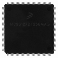
MC9S12XDT256MAG Freescale Semiconductor, MC9S12XDT256MAG Datasheet - Page 511

MC9S12XDT256MAG
Manufacturer Part Number
MC9S12XDT256MAG
Description
IC MCU 256K FLASH 144-LQFP
Manufacturer
Freescale Semiconductor
Series
HCS12r
Datasheet
1.MC9S12XD64CAA.pdf
(1348 pages)
Specifications of MC9S12XDT256MAG
Core Processor
HCS12X
Core Size
16-Bit
Speed
80MHz
Connectivity
CAN, EBI/EMI, I²C, IrDA, LIN, SCI, SPI
Peripherals
LVD, POR, PWM, WDT
Number Of I /o
119
Program Memory Size
256KB (256K x 8)
Program Memory Type
FLASH
Eeprom Size
4K x 8
Ram Size
16K x 8
Voltage - Supply (vcc/vdd)
2.35 V ~ 5.5 V
Data Converters
A/D 24x10b
Oscillator Type
External
Operating Temperature
-40°C ~ 125°C
Package / Case
144-LQFP
Processor Series
S12XD
Core
HCS12
Data Bus Width
16 bit
Data Ram Size
16 KB
Interface Type
CAN/I2C/SCI/SPI
Maximum Clock Frequency
40 MHz
Number Of Programmable I/os
119
Number Of Timers
12
Operating Supply Voltage
0 V to 5.5 V
Maximum Operating Temperature
+ 125 C
Mounting Style
SMD/SMT
3rd Party Development Tools
EWHCS12
Development Tools By Supplier
EVB9S12XDP512E
Minimum Operating Temperature
- 40 C
On-chip Adc
2 (24-ch x 10-bit)
Lead Free Status / RoHS Status
Lead free / RoHS Compliant
Available stocks
Company
Part Number
Manufacturer
Quantity
Price
Company:
Part Number:
MC9S12XDT256MAG
Manufacturer:
Freescale Semiconductor
Quantity:
10 000
- Current page: 511 of 1348
- Download datasheet (8Mb)
Enable single-wire operation by setting the LOOPS bit and the receiver source bit, RSRC, in SCI control
register 1 (SCICR1). Setting the LOOPS bit disables the path from the RXD pin to the receiver. Setting
the RSRC bit connects the TXD pin to the receiver. Both the transmitter and receiver must be enabled
(TE = 1 and RE = 1).The TXDIR bit (SCISR2[1]) determines whether the TXD pin is going to be used as
an input (TXDIR = 0) or an output (TXDIR = 1) in this mode of operation.
11.4.8
In loop operation the transmitter output goes to the receiver input. The RXD pin is disconnected from the
SCI.
Enable loop operation by setting the LOOPS bit and clearing the RSRC bit in SCI control register 1
(SCICR1). Setting the LOOPS bit disables the path from the RXD pin to the receiver. Clearing the RSRC
bit connects the transmitter output to the receiver input. Both the transmitter and receiver must be enabled
(TE = 1 and RE = 1).
11.5
11.5.1
See
11.5.2
11.5.2.1
Normal mode of operation.
To initialize a SCI transmission, see
Freescale Semiconductor
Section 11.3.2, “Register
Initialization/Application Information
Loop Operation
Reset Initialization
Modes of Operation
Run Mode
In single-wire operation data from the TXD pin is inverted if RXPOL is set.
In loop operation data from the transmitter is not recognized by the receiver
if RXPOL and TXPOL are not the same.
Figure 11-31. Loop Operation (LOOPS = 1, RSRC = 0)
Descriptions”.
Transmitter
MC9S12XDP512 Data Sheet, Rev. 2.21
Section 11.4.5.2, “Character
Receiver
NOTE
NOTE
Chapter 11 Serial Communication Interface (S12SCIV5)
Transmission”.
RXD
TXD
511
Related parts for MC9S12XDT256MAG
Image
Part Number
Description
Manufacturer
Datasheet
Request
R

Part Number:
Description:
16-BIT MICROPROCESSOR FAMILY
Manufacturer:
FREESCALE [Freescale Semiconductor, Inc]
Datasheet:
Part Number:
Description:
Manufacturer:
Freescale Semiconductor, Inc
Datasheet:
Part Number:
Description:
Manufacturer:
Freescale Semiconductor, Inc
Datasheet:
Part Number:
Description:
Manufacturer:
Freescale Semiconductor, Inc
Datasheet:
Part Number:
Description:
Manufacturer:
Freescale Semiconductor, Inc
Datasheet:
Part Number:
Description:
Manufacturer:
Freescale Semiconductor, Inc
Datasheet:
Part Number:
Description:
Manufacturer:
Freescale Semiconductor, Inc
Datasheet:
Part Number:
Description:
Manufacturer:
Freescale Semiconductor, Inc
Datasheet:
Part Number:
Description:
Manufacturer:
Freescale Semiconductor, Inc
Datasheet:
Part Number:
Description:
Manufacturer:
Freescale Semiconductor, Inc
Datasheet:
Part Number:
Description:
Manufacturer:
Freescale Semiconductor, Inc
Datasheet:
Part Number:
Description:
Manufacturer:
Freescale Semiconductor, Inc
Datasheet:
Part Number:
Description:
Manufacturer:
Freescale Semiconductor, Inc
Datasheet:
Part Number:
Description:
Manufacturer:
Freescale Semiconductor, Inc
Datasheet:
Part Number:
Description:
Manufacturer:
Freescale Semiconductor, Inc
Datasheet:


