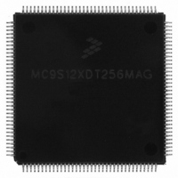
MC9S12XDT256MAG Freescale Semiconductor, MC9S12XDT256MAG Datasheet - Page 1235

MC9S12XDT256MAG
Manufacturer Part Number
MC9S12XDT256MAG
Description
IC MCU 256K FLASH 144-LQFP
Manufacturer
Freescale Semiconductor
Series
HCS12r
Datasheet
1.MC9S12XD64CAA.pdf
(1348 pages)
Specifications of MC9S12XDT256MAG
Core Processor
HCS12X
Core Size
16-Bit
Speed
80MHz
Connectivity
CAN, EBI/EMI, I²C, IrDA, LIN, SCI, SPI
Peripherals
LVD, POR, PWM, WDT
Number Of I /o
119
Program Memory Size
256KB (256K x 8)
Program Memory Type
FLASH
Eeprom Size
4K x 8
Ram Size
16K x 8
Voltage - Supply (vcc/vdd)
2.35 V ~ 5.5 V
Data Converters
A/D 24x10b
Oscillator Type
External
Operating Temperature
-40°C ~ 125°C
Package / Case
144-LQFP
Processor Series
S12XD
Core
HCS12
Data Bus Width
16 bit
Data Ram Size
16 KB
Interface Type
CAN/I2C/SCI/SPI
Maximum Clock Frequency
40 MHz
Number Of Programmable I/os
119
Number Of Timers
12
Operating Supply Voltage
0 V to 5.5 V
Maximum Operating Temperature
+ 125 C
Mounting Style
SMD/SMT
3rd Party Development Tools
EWHCS12
Development Tools By Supplier
EVB9S12XDP512E
Minimum Operating Temperature
- 40 C
On-chip Adc
2 (24-ch x 10-bit)
Lead Free Status / RoHS Status
Lead free / RoHS Compliant
Available stocks
Company
Part Number
Manufacturer
Quantity
Price
Company:
Part Number:
MC9S12XDT256MAG
Manufacturer:
Freescale Semiconductor
Quantity:
10 000
- Current page: 1235 of 1348
- Download datasheet (8Mb)
Special single chip erase and unsecure sequence:
Freescale Semiconductor
1. Reset into special single chip mode.
2. Write an appropriate value to the ECLKDIV register for correct timing.
3. Write 0xFF to the EPROT register to disable protection.
4. Write 0x30 to the ESTAT register to clear the PVIOL and ACCERR bits.
5. Write 0x0000 to the EDATA register (0x011A–0x011B).
6. Write 0x0000 to the EADDR register (0x0118–0x0119).
7. Write 0x41 (mass erase) to the ECMD register.
8. Write 0x80 to the ESTAT register to clear CBEIF.
9. Write an appropriate value to the FCLKDIV register for correct timing.
10. Write 0x00 to the FCNFG register to select Flash block 0.
11. Write 0x10 to the FTSTMOD register (0x0102) to set the WRALL bit, so the following writes
12. Write 0xFF to the FPROT register to disable protection.
13. Write 0x30 to the FSTAT register to clear the PVIOL and ACCERR bits.
14. Write 0x0000 to the FDATA register (0x010A–0x010B).
15. Write 0x0000 to the FADDR register (0x0108–0x0109).
16. Write 0x41 (mass erase) to the FCMD register.
17. Write 0x80 to the FSTAT register to clear CBEIF.
18. Wait until all CCIF flags are set.
19. Reset back into special single chip mode.
20. Write an appropriate value to the FCLKDIV register for correct timing.
21. Write 0x00 to the FCNFG register to select Flash block 0.
22. Write 0xFF to the FPROT register to disable protection.
23. Write 0xFFBE to Flash address 0xFF0E.
24. Write 0x20 (program) to the FCMD register.
25. Write 0x80 to the FSTAT register to clear CBEIF.
26. Wait until the CCIF flag in FSTAT is are set.
27. Reset into any mode.
affect all Flash blocks.
MC9S12XDP512 Data Sheet, Rev. 2.21
Chapter 30 Security (S12X9SECV2)
1237
Related parts for MC9S12XDT256MAG
Image
Part Number
Description
Manufacturer
Datasheet
Request
R

Part Number:
Description:
16-BIT MICROPROCESSOR FAMILY
Manufacturer:
FREESCALE [Freescale Semiconductor, Inc]
Datasheet:
Part Number:
Description:
Manufacturer:
Freescale Semiconductor, Inc
Datasheet:
Part Number:
Description:
Manufacturer:
Freescale Semiconductor, Inc
Datasheet:
Part Number:
Description:
Manufacturer:
Freescale Semiconductor, Inc
Datasheet:
Part Number:
Description:
Manufacturer:
Freescale Semiconductor, Inc
Datasheet:
Part Number:
Description:
Manufacturer:
Freescale Semiconductor, Inc
Datasheet:
Part Number:
Description:
Manufacturer:
Freescale Semiconductor, Inc
Datasheet:
Part Number:
Description:
Manufacturer:
Freescale Semiconductor, Inc
Datasheet:
Part Number:
Description:
Manufacturer:
Freescale Semiconductor, Inc
Datasheet:
Part Number:
Description:
Manufacturer:
Freescale Semiconductor, Inc
Datasheet:
Part Number:
Description:
Manufacturer:
Freescale Semiconductor, Inc
Datasheet:
Part Number:
Description:
Manufacturer:
Freescale Semiconductor, Inc
Datasheet:
Part Number:
Description:
Manufacturer:
Freescale Semiconductor, Inc
Datasheet:
Part Number:
Description:
Manufacturer:
Freescale Semiconductor, Inc
Datasheet:
Part Number:
Description:
Manufacturer:
Freescale Semiconductor, Inc
Datasheet:


