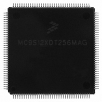
MC9S12XDT256MAG Freescale Semiconductor, MC9S12XDT256MAG Datasheet - Page 1005

MC9S12XDT256MAG
Manufacturer Part Number
MC9S12XDT256MAG
Description
IC MCU 256K FLASH 144-LQFP
Manufacturer
Freescale Semiconductor
Series
HCS12r
Datasheet
1.MC9S12XD64CAA.pdf
(1348 pages)
Specifications of MC9S12XDT256MAG
Core Processor
HCS12X
Core Size
16-Bit
Speed
80MHz
Connectivity
CAN, EBI/EMI, I²C, IrDA, LIN, SCI, SPI
Peripherals
LVD, POR, PWM, WDT
Number Of I /o
119
Program Memory Size
256KB (256K x 8)
Program Memory Type
FLASH
Eeprom Size
4K x 8
Ram Size
16K x 8
Voltage - Supply (vcc/vdd)
2.35 V ~ 5.5 V
Data Converters
A/D 24x10b
Oscillator Type
External
Operating Temperature
-40°C ~ 125°C
Package / Case
144-LQFP
Processor Series
S12XD
Core
HCS12
Data Bus Width
16 bit
Data Ram Size
16 KB
Interface Type
CAN/I2C/SCI/SPI
Maximum Clock Frequency
40 MHz
Number Of Programmable I/os
119
Number Of Timers
12
Operating Supply Voltage
0 V to 5.5 V
Maximum Operating Temperature
+ 125 C
Mounting Style
SMD/SMT
3rd Party Development Tools
EWHCS12
Development Tools By Supplier
EVB9S12XDP512E
Minimum Operating Temperature
- 40 C
On-chip Adc
2 (24-ch x 10-bit)
Lead Free Status / RoHS Status
Lead free / RoHS Compliant
Available stocks
Company
Part Number
Manufacturer
Quantity
Price
Company:
Part Number:
MC9S12XDT256MAG
Manufacturer:
Freescale Semiconductor
Quantity:
10 000
- Current page: 1005 of 1348
- Download datasheet (8Mb)
WOMS[7:0]
Routed
Routed
Routed
PTM[7:6]
PTM[5:4]
CAN0
CAN4
Reset
This register configures the output pins as wired-OR. If enabled the output is driven active low only
(open-drain). A logic level of “1” is not driven. It applies also to the SPI and SCI outputs and allows
a multipoint connection of several serial modules. These bits have no influence on pins used as
inputs.
Field
24.0.5.26 Port M Data Register (PTM)
Read: Anytime.
Write: Anytime.
Port M pins 7–0 are associated with the CAN0, as well as the routed CAN0, CAN4, and SPI0
modules. When not used with any of the peripherals, these pins can be used as general purpose I/O.
If the data direction bits of the associated I/O pins are set to logic level “1”, a read returns the value
of the port register, otherwise the buffered pin input state is read.
Field
CAN
SPI0
7–0
7–6
5–4
W
R
TXCAN4
PTM7
Wired-OR Mode Port S
0 Output buffers operate as push-pull outputs.
1 Output buffers operate as open-drain outputs.
The CAN4 function (TXCAN4 and RXCAN4) takes precedence over the general purpose I/O function if the CAN4
module is enabled. Refer to MSCAN section for details.
The routed CAN0 function (TXCAN0 and RXCAN0) takes precedence over the routed CAN4, the routed SPI0
and the general purpose I/O function if the routed CAN0 module is enabled.
The routed CAN4 function (TXCAN4 and RXCAN4) takes precedence over the routed SPI0 and general purpose
I/O function if the routed CAN4 module is enabled. Refer to MSCAN section for details.
The routed SPI0 function (SCK0 and MOSI0) takes precedence of the general purpose I/O function if the routed
SPI0 is enabled. Refer to SPI section for details.
7
0
RXCAN4
PTM6
0
6
Figure 24-28. Port M Data Register (PTM)
Table 24-27. WOMS Field Descriptions
Table 24-28. PTM Field Descriptions
TXCAN0
TXCAN4
PTM5
SCK0
5
0
RXCAN0
RXCAN4
MOSI0
PTM4
0
4
Description
Description
TXCAN0
PTM3
SS0
3
0
RXCAN0
MISO0
PTM2
0
2
TXCAN0
PTM1
1
0
RXCAN0
PTM0
0
0
Related parts for MC9S12XDT256MAG
Image
Part Number
Description
Manufacturer
Datasheet
Request
R

Part Number:
Description:
16-BIT MICROPROCESSOR FAMILY
Manufacturer:
FREESCALE [Freescale Semiconductor, Inc]
Datasheet:
Part Number:
Description:
Manufacturer:
Freescale Semiconductor, Inc
Datasheet:
Part Number:
Description:
Manufacturer:
Freescale Semiconductor, Inc
Datasheet:
Part Number:
Description:
Manufacturer:
Freescale Semiconductor, Inc
Datasheet:
Part Number:
Description:
Manufacturer:
Freescale Semiconductor, Inc
Datasheet:
Part Number:
Description:
Manufacturer:
Freescale Semiconductor, Inc
Datasheet:
Part Number:
Description:
Manufacturer:
Freescale Semiconductor, Inc
Datasheet:
Part Number:
Description:
Manufacturer:
Freescale Semiconductor, Inc
Datasheet:
Part Number:
Description:
Manufacturer:
Freescale Semiconductor, Inc
Datasheet:
Part Number:
Description:
Manufacturer:
Freescale Semiconductor, Inc
Datasheet:
Part Number:
Description:
Manufacturer:
Freescale Semiconductor, Inc
Datasheet:
Part Number:
Description:
Manufacturer:
Freescale Semiconductor, Inc
Datasheet:
Part Number:
Description:
Manufacturer:
Freescale Semiconductor, Inc
Datasheet:
Part Number:
Description:
Manufacturer:
Freescale Semiconductor, Inc
Datasheet:
Part Number:
Description:
Manufacturer:
Freescale Semiconductor, Inc
Datasheet:


