EVAL-ADUC814QS Analog Devices Inc, EVAL-ADUC814QS Datasheet - Page 62
EVAL-ADUC814QS
Manufacturer Part Number
EVAL-ADUC814QS
Description
KIT DEV FOR ADUC814 QUICK START
Manufacturer
Analog Devices Inc
Series
QuickStart™ Kitr
Type
8052-corer
Datasheet
1.EVAL-ADUC814QSZ.pdf
(72 pages)
Specifications of EVAL-ADUC814QS
Contents
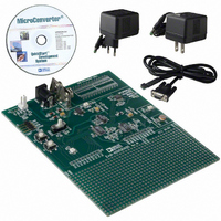
Evaluation Board, Power Supply, Cable, Software and Documentation
For Use With/related Products
ADuC814
Lead Free Status / RoHS Status
Contains lead / RoHS non-compliant


ADuC814
In all of these scenarios, and in more complicated real-life appli-
cations, keep in mind the flow of current from the supplies and
back to ground. Make sure the return paths for all currents are
as close as possible to the paths the currents took to reach their
destinations. For example, do not put power components on the
analog side of Figure 58b with DV
return currents from DV
avoid digital currents flowing under analog circuitry, which
could happen if a noisy digital chip is placed on the left half of
the board in Figure 58c. Whenever possible, avoid large
discontinuities in the ground plane(s) (such as are formed by a
long trace on the same layer), because they force return signals
to travel a longer path. And of course, make all connections to
the ground plane directly, with little or no trace separating the
pin from its via to ground.
If the user plans to connect fast logic signals (rise/fall time
< 5 ns) to any of the ADuC814’s digital inputs, add a series
resistor to each relevant line to keep rise and fall times longer
than 5 ns at the ADuC814 input pins. A value of 100 Ω or 200 Ω
is usually sufficient to prevent high speed signals from coupling
capacitively into the ADuC814 and affecting the accuracy of
ADC conversions.
a.
b.
c.
PLACE ANALOG
COMPONENTS
PLACE ANALOG
COMPONENTS
HERE
PLACE ANALOG
AGND
AGND
COMPONENTS
Figure 58. System Grounding Schemes
HERE
HERE
DD
to flow through AGND. Also, try to
GND
DD
because that would force
PLACE DIGITAL
COMPONENTS
PLACE DIGITAL
COMPONENTS
PLACE DIGITAL
COMPONENTS
HERE
HERE
HERE
DGND
DGND
Rev. A | Page 62 of 72
OTHER HARDWARE CONSIDERATIONS
To facilitate in-circuit programming, in-circuit debug, and
emulation options, users should implement some simple
connection points in their hardware. A typical ADuC814
connection diagram is shown in Figure 59.
In-Circuit Serial Download Access
Nearly all ADuC814 designs will want to take advantage of the
in-circuit reprogrammability of the chip. This is accomplished
by a connection from the ADuC814’s UART to a PC, which
requires an external RS-232 chip for level translation. If users
would rather not design an RS-232 chip onto a board, refer to
the Application Note uC006, A 4-Wire UART-to-PC Interface
(available at www.analog.com/microconverter) for a simple
(and zero-cost-per-board) method of gaining in-circuit serial
download access to the ADuC814.
In addition to the basic UART connections, users also need a
way to trigger the chip into download mode. This is accom-
plished via a 1 kΩ pull-up resistor that can be jumpered onto
the DLOAD pin. To get the ADuC814 into download mode,
simply connect this jumper and power-cycle the device (or
manually reset the device, if a manual reset button is available),
and it will be ready to receive a new program serially. To enable
the device to enter normal mode (and run the program) when-
ever power is cycled or RESET is toggled, the DLOAD pin must
be pulled low through a 1 kΩ resistor.
Embedded Serial Port Debugger
From a hardware perspective, entry to serial port debug mode is
identical to the serial download entry sequence described in the
preceding section. In fact, both serial download and serial port
debug modes can be thought of as essentially one mode of
operation used in two different ways. Note that the serial port
debugger is fully contained on the ADuC814 device, unlike
ROM monitor type debuggers.
Related parts for EVAL-ADUC814QS
Image
Part Number
Description
Manufacturer
Datasheet
Request
R


Part Number:
Description:
BOARD EVAL FOR SI270X-A
Manufacturer:
Silicon Laboratories Inc
Datasheet:

Part Number:
Description:
BUCK CONV REF DESIGN KIT IP1201
Manufacturer:
International Rectifier
Datasheet:
Part Number:
Description:
BOARD DEMO SYNC DUAL BUCK CNVTER
Manufacturer:
International Rectifier
Datasheet:
Part Number:
Description:
BOARD DEMO SYNC BUCK CONVETER
Manufacturer:
International Rectifier
Datasheet:

Part Number:
Description:
EVALBOARD/EB Omnidirectional microphone - Analog
Manufacturer:
Analog Devices
Datasheet:
Part Number:
Description:
EVALBOARD/EB Omnidirectional microphone - Analog
Manufacturer:
Analog Devices
Datasheet:


Part Number:
Description:
BOARD EVAL LED DRIVER LT3756
Manufacturer:
Linear Technology
Datasheet:

Part Number:
Description:
BOARD EVAL FOR AD7741/7742
Manufacturer:
Analog Devices Inc
Datasheet:

Part Number:
Description:
±1.7g Dual-Axis IMEMS Accelerometer Evaluation Board
Manufacturer:
Analog Devices Inc
Datasheet:

Part Number:
Description:
IC MULTIPLIER ANALOG 8-SOIC T/R
Manufacturer:
Analog Devices Inc
Datasheet:

Part Number:
Description:
IC ANALOG MULTIPLIER 8-DIP
Manufacturer:
Analog Devices Inc
Datasheet:
Part Number:
Description:
IC ANALOG MULTIPLIER 8-SOIC
Manufacturer:
Analog Devices Inc
Datasheet:
Part Number:
Description:
IC ANALOG MULTIPLIER 8-DIP
Manufacturer:
Analog Devices Inc
Datasheet: