EVAL-ADUC814QS Analog Devices Inc, EVAL-ADUC814QS Datasheet - Page 61
EVAL-ADUC814QS
Manufacturer Part Number
EVAL-ADUC814QS
Description
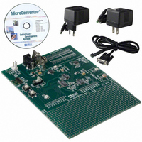
KIT DEV FOR ADUC814 QUICK START
Manufacturer
Analog Devices Inc
Series
QuickStart™ Kitr
Type
8052-corer
Datasheet
1.EVAL-ADUC814QSZ.pdf
(72 pages)
Specifications of EVAL-ADUC814QS
Contents
Evaluation Board, Power Supply, Cable, Software and Documentation
For Use With/related Products
ADuC814
Lead Free Status / RoHS Status
Contains lead / RoHS non-compliant


Power-Saving Modes
Setting the idle and power-down mode bits, PCON.0 and
PCON.1, respectively, in the PCON SFR described in Table 5,
allows the chip to be switched from normal mode to idle mode,
and also to full power-down mode.
In idle mode, the oscillator continues to run, but the core clock
generated from the PLL is halted. The on-chip peripherals con-
tinue to receive the clock and remain functional. The CPU status
is preserved with the stack pointer, program counter, and all
other internal registers maintaining their data during idle mode.
Port pins and DAC output pins also retain their states in this
mode. The chip recovers from idle mode upon receiving any
enabled interrupt, or upon receiving a hardware reset.
In power-down mode, both the PLL and the clock to the core
are stopped. The on-chip oscillator can be halted or can
continue to oscillate depending on the state of the oscillator
power-down bit (OSC_PD) in the PLLCON SFR. The TIC,
being driven directly from the oscillator, can also be enabled
during power-down. All other on-chip peripherals however, are
shut down. Port pins retain their logic levels in this mode, but
the DAC output goes to a high impedance state (three-state).
During full power-down mode, the ADuC814 consumes a total
of 5 µA typically. There are five ways of terminating power-
down mode, as described in the next sections.
Asserting RESET (Pin 10)
Returns to normal mode and all registers are set to their default
state. Program execution starts at the reset vector once the RESET
pin is de-asserted.
Cycling Power
All registers are set to their default state and program execution
starts at the reset vector.
Time Interval Counter (TIC) Interrupt
Power-down mode is terminated and the CPU services the TIC
interrupt. The RETI at the end of the TIC interrupt service
routine returns the core to the instruction following the one
that enabled power-down.
SPI Interrupt
Power-down mode is terminated and the CPU services the SPI
interrupt. The RETI at the end of the ISR returns the core to the
instruction following the one that enabled power-down. Note
that the SPI power-down interrupt enable bit (SERIPD) in the
PCON SFR must first be set to allow this mode of operation.
Rev. A | Page 61 of 72
INT0 Interrupt
Power-down mode is terminated and the CPU services the
INT0 interrupt. The RETI at the end of the ISR returns the core
to the instruction following the one that enabled power-down.
The INT0 pin must not be driven low during or within two
machine cycles of the instruction that initiates power-down
mode. Note that the INT0 power-down interrupt enable bit
(INT0PD) in the PCON SFR must first be set to allow this mode
of operation.
Power-On Reset
An internal POR (power-on-reset) is implemented on the
ADuC814. For DV
ADuC814 in reset. As DV
times out for approximately128 ms before the part is released
from reset. The user must ensure that the power supply has
reached a stable 2.7 V minimum level by this time. Likewise on
power-down, the internal POR holds the ADuC814 in reset
until the power supply has dropped below 1 V. Figure 57
illustrates the operation of the internal POR in detail.
Grounding and Board Layout Recommendations
As with all high resolution data converters, special attention
must be paid to grounding and PC board layout of ADuC814
based designs in order to achieve optimum performance from
the ADCs and DAC. Although the ADuC814 has separate pins
for analog and digital ground (AGND and DGND), the user
must not tie these to two separate ground planes unless the two
ground planes are connected together very close to the ADuC814,
as illustrated in the simplified example of Figure 58a. In systems
where digital and analog ground planes are connected together
somewhere else (at the system’s power supply for example), they
cannot be connected again near the ADuC814 because a ground
loop would result. In these cases, tie all of the ADuC814’s
AGND and DGND pins to the analog ground plane, as
illustrated in Figure 58b. In systems with only one ground plane,
ensure that the digital and analog components are physically
separated onto separate halves of the board such that digital
return currents do not flow near analog circuitry and vice versa.
The ADuC814 can then be placed between the digital and
analog sections, as illustrated in Figure 58c.
DV
CORE RESET
INTERNAL
DD
2.45V TYP
1.0V TYP
Figure 57. Internal POR Operation
DD
128ms TYP
below 2.45 V, the internal POR holds the
DD
rises above 2.45 V, an internal timer
128ms TYP
ADuC814
1.0V
Related parts for EVAL-ADUC814QS
Image
Part Number
Description
Manufacturer
Datasheet
Request
R


Part Number:
Description:
BOARD EVAL FOR SI270X-A
Manufacturer:
Silicon Laboratories Inc
Datasheet:

Part Number:
Description:
BUCK CONV REF DESIGN KIT IP1201
Manufacturer:
International Rectifier
Datasheet:
Part Number:
Description:
BOARD DEMO SYNC DUAL BUCK CNVTER
Manufacturer:
International Rectifier
Datasheet:
Part Number:
Description:
BOARD DEMO SYNC BUCK CONVETER
Manufacturer:
International Rectifier
Datasheet:

Part Number:
Description:
EVALBOARD/EB Omnidirectional microphone - Analog
Manufacturer:
Analog Devices
Datasheet:
Part Number:
Description:
EVALBOARD/EB Omnidirectional microphone - Analog
Manufacturer:
Analog Devices
Datasheet:


Part Number:
Description:
BOARD EVAL LED DRIVER LT3756
Manufacturer:
Linear Technology
Datasheet:

Part Number:
Description:
BOARD EVAL FOR AD7741/7742
Manufacturer:
Analog Devices Inc
Datasheet:

Part Number:
Description:
±1.7g Dual-Axis IMEMS Accelerometer Evaluation Board
Manufacturer:
Analog Devices Inc
Datasheet:

Part Number:
Description:
IC MULTIPLIER ANALOG 8-SOIC T/R
Manufacturer:
Analog Devices Inc
Datasheet:

Part Number:
Description:
IC ANALOG MULTIPLIER 8-DIP
Manufacturer:
Analog Devices Inc
Datasheet:
Part Number:
Description:
IC ANALOG MULTIPLIER 8-SOIC
Manufacturer:
Analog Devices Inc
Datasheet:
Part Number:
Description:
IC ANALOG MULTIPLIER 8-DIP
Manufacturer:
Analog Devices Inc
Datasheet: