EVAL-ADUC814QS Analog Devices Inc, EVAL-ADUC814QS Datasheet - Page 30
EVAL-ADUC814QS
Manufacturer Part Number
EVAL-ADUC814QS
Description
KIT DEV FOR ADUC814 QUICK START
Manufacturer
Analog Devices Inc
Series
QuickStart™ Kitr
Type
8052-corer
Datasheet
1.EVAL-ADUC814QSZ.pdf
(72 pages)
Specifications of EVAL-ADUC814QS
Contents
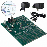
Evaluation Board, Power Supply, Cable, Software and Documentation
For Use With/related Products
ADuC814
Lead Free Status / RoHS Status
Contains lead / RoHS non-compliant


ADuC814
NONVOLITILE FLASH/EE MEMORY
FLASH/EE MEMORY OVERVIEW
The ADuC814 incorporates Flash/EE memory technology on-
chip to provide the user with nonvolatile, in-circuit reprogram-
mable code and data memory space.
Flash/EE memory takes the flexible in-circuit reprogrammable
features of EEPROM and combines them with the space efficient/
density features of EPROM (see Figure 32).
Because Flash/EE technology is based on a single transistor cell
architecture, a Flash memory array such as EPROM can be
implemented to achieve the space efficiencies or memory
densities required by a given design.
Like EEPROM, flash memory can be programmed in-system at
a byte level, although it must first be erased; the erase being
performed in page blocks. Thus, flash memory is often and
more correctly referred to as Flash/EE memory.
Incorporated in the ADuC814, Flash/EE memory technology
allows the user to update program code space in-circuit without
the need to replace one-time programmable (OTP) devices at
remote operating nodes.
FLASH/EE MEMORY AND THE ADUC814
The ADuC814 provides two arrays of Flash/EE memory for
user applications. There are 8 kbytes of Flash/EE program space
provided on-chip to facilitate code execution, therefore removing
the requirement for an external discrete ROM device. The pro-
gram memory can be programmed using conventional third-
party memory programmers. This array can also be programmed
in-circuit, using the serial download mode provided.
A 640-byte Flash/EE data memory space is also provided on-
chip. This may be used as a general-purpose nonvolatile
scratchpad area. User access to this area is via a group of six
SFRs. This space can be programmed at a byte level, although it
must first be erased in 4-byte pages.
ADUC814 FLASH/EE MEMORY RELIABILITY
The Flash/EE program and data memory arrays on the
ADuC814 are fully qualified for two key Flash/EE memory
characteristics: Flash/EE memory cycling endurance and
Flash/EE memory data retention.
SPACE EFFICIENT/
DENSITY
TECHNOLOGY
Figure 32. Flash/EE Memory Development
EPROM
FLASH/EE MEMORY
TECHNOLOGY
TECHNOLOGY
REPROGRAMMABLE
EEPROM
IN-CIRCUIT
Rev. A | Page 30 of 72
Endurance quantifies the ability of the Flash/EE memory to be
cycled through many program, read, and erase cycles. In real
terms, a single endurance cycle is composed of four
independent, sequential events:
1.
2.
3.
4.
In reliability qualification, every byte in both the program and
data Flash/EE memory is cycled from 00H to FFH until a first
fail is recorded signifying the endurance limit of the on-chip
Flash/EE memory.
As indicated in the Specifications tables, the ADuC814 Flash/EE
memory endurance qualification has been carried out in accor-
dance with JEDEC Specification A117 over the industrial
temperature range of –40°C to +125°C. The results allow the
specification of a minimum endurance figure over supply and a
temperature of 100,000 cycles, with an endurance figure of
700,000 cycles being typical of operation at 25°C.
Retention quantifies the ability of the Flash/EE memory to
retain its programmed data over time. Again, the ADuC814 has
been qualified in accordance with the formal JEDEC Retention
Lifetime Specification (A117) at a specific junction temperature
(T
memory is cycled to its specified endurance limit described
above, before data retention is characterized. This means that
the Flash/EE memory is guaranteed to retain its data for its full
specified retention lifetime every time the Flash/EE memory is
reprogrammed. It should be noted that retention lifetime, based
on an activation energy of 0.6 eV, derates with T
Figure 33.
J
= 55°C). As part of this qualification procedure, the Flash/EE
Initial page erase sequence
Read/verify sequence
Byte program sequence
Second read/verify sequence
300
250
200
150
100
50
0
40
Figure 33. Flash/EE Memory Data Retention
50
T
J
60
JUNCTION TEMPERATURE (°C)
ADI SPECIFICATION
100 YEARS MIN.
AT T
70
J
= 55°C
80
90
J
as shown in
100
110
Related parts for EVAL-ADUC814QS
Image
Part Number
Description
Manufacturer
Datasheet
Request
R


Part Number:
Description:
BOARD EVAL FOR SI270X-A
Manufacturer:
Silicon Laboratories Inc
Datasheet:

Part Number:
Description:
BUCK CONV REF DESIGN KIT IP1201
Manufacturer:
International Rectifier
Datasheet:
Part Number:
Description:
BOARD DEMO SYNC DUAL BUCK CNVTER
Manufacturer:
International Rectifier
Datasheet:
Part Number:
Description:
BOARD DEMO SYNC BUCK CONVETER
Manufacturer:
International Rectifier
Datasheet:

Part Number:
Description:
EVALBOARD/EB Omnidirectional microphone - Analog
Manufacturer:
Analog Devices
Datasheet:
Part Number:
Description:
EVALBOARD/EB Omnidirectional microphone - Analog
Manufacturer:
Analog Devices
Datasheet:


Part Number:
Description:
BOARD EVAL LED DRIVER LT3756
Manufacturer:
Linear Technology
Datasheet:

Part Number:
Description:
BOARD EVAL FOR AD7741/7742
Manufacturer:
Analog Devices Inc
Datasheet:

Part Number:
Description:
±1.7g Dual-Axis IMEMS Accelerometer Evaluation Board
Manufacturer:
Analog Devices Inc
Datasheet:

Part Number:
Description:
IC MULTIPLIER ANALOG 8-SOIC T/R
Manufacturer:
Analog Devices Inc
Datasheet:

Part Number:
Description:
IC ANALOG MULTIPLIER 8-DIP
Manufacturer:
Analog Devices Inc
Datasheet:
Part Number:
Description:
IC ANALOG MULTIPLIER 8-SOIC
Manufacturer:
Analog Devices Inc
Datasheet:
Part Number:
Description:
IC ANALOG MULTIPLIER 8-DIP
Manufacturer:
Analog Devices Inc
Datasheet: