MC56F8323EVME Freescale Semiconductor, MC56F8323EVME Datasheet - Page 21
MC56F8323EVME
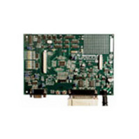
Manufacturer Part Number
MC56F8323EVME
Description
BOARD EVALUATION MC56F8323
Manufacturer
Freescale Semiconductor
Type
DSPr
Specifications of MC56F8323EVME
Contents
Module and Misc Hardware
Processor To Be Evaluated
MC56F8322 and MC56F8323
Data Bus Width
16 bit
Interface Type
RS-232
Silicon Manufacturer
Freescale
Core Architecture
56800/E
Core Sub-architecture
56800/E
Silicon Core Number
MC56F
Silicon Family Name
MC56F83xx
Rohs Compliant
Yes
For Use With/related Products
MC56F8322, MC56F8323
Lead Free Status / RoHS Status
Lead free / RoHS Compliant


Freescale Semiconductor
Preliminary
Signal Name
(oscillator_
PHASEA0
(GPIOB7)
clock)
TRST
(TA0)
TMS
TDO
TDI
Table 2-2 Signal and Package Information for the 64-Pin LQFP
Pin No.
54
55
56
58
52
Schmitt
Schmitt
Schmitt
Schmitt
Schmitt
Schmitt
Output
Output
Output
Output
Input/
Input/
Type
Input
Input
Input
Input
State During
pulled high
pulled high
pulled high
internally
internally
disabled,
pull-up is
internally
output is
In reset,
enabled
enabled
pull-up
Reset
56F8323 Technical Data, Rev. 17
Input,
Input,
Input,
Input,
Test Mode Select Input — This input pin is used to sequence the
JTAG TAP controller’s state machine. It is sampled on the rising
edge of TCK and has an on-chip pull-up resistor.
Note:
Test Data Input — This input pin provides a serial input data stream
to the JTAG/EOnCE port. It is sampled on the rising edge of TCK and
has an on-chip pull-up resistor.
Test Data Output — This tri-stateable output pin provides a serial
output data stream from the JTAG/EOnCE port. It is driven in the
shift-IR and shift-DR controller states, and changes on the falling
edge of TCK.
Test Reset — As an input, a low signal on this pin provides a reset
signal to the JTAG TAP controller. To ensure complete hardware
reset, TRST should be asserted whenever RESET is asserted. The
only exception occurs in a debugging environment when a hardware
device reset is required and the EOnCE/JTAG module must not be
reset. In this case, assert RESET, but do not assert TRST.
To deactivate the internal pull-up resistor, set the JTAG bit in the
SIM_PUDR register.
Note:
is to be used in a debugging environment, TRST may be tied to V
a 1K resistor.
Phase A — Quadrature Decoder 0, PHASEA input
TA0 — Timer A, Channel 0
Port B GPIO — This GPIO pin can be individually programmed as
an input or output pin.
Clock Output - can be used to monitor the internal oscillator clock
signal (see
In the 56F8323, the default state after reset is PHASEA0.
In the 56F8123, the default state is not one of the functions offered
and must be reconfigured.
Always tie the TMS pin to V
For normal operation, connect TRST directly to V
Part 6.5.7
CLKO Select Register, SIM_CLKOSR).
Signal Description
DD
through a 2.2K resistor.
SS
. If the design
SS
Signal Pins
through
21
Related parts for MC56F8323EVME
Image
Part Number
Description
Manufacturer
Datasheet
Request
R

Part Number:
Description:
Manufacturer:
Freescale Semiconductor, Inc
Datasheet:
Part Number:
Description:
Manufacturer:
Freescale Semiconductor, Inc
Datasheet:
Part Number:
Description:
Manufacturer:
Freescale Semiconductor, Inc
Datasheet:
Part Number:
Description:
Manufacturer:
Freescale Semiconductor, Inc
Datasheet:
Part Number:
Description:
Manufacturer:
Freescale Semiconductor, Inc
Datasheet:
Part Number:
Description:
Manufacturer:
Freescale Semiconductor, Inc
Datasheet:
Part Number:
Description:
Manufacturer:
Freescale Semiconductor, Inc
Datasheet:
Part Number:
Description:
Manufacturer:
Freescale Semiconductor, Inc
Datasheet:
Part Number:
Description:
Manufacturer:
Freescale Semiconductor, Inc
Datasheet:
Part Number:
Description:
Manufacturer:
Freescale Semiconductor, Inc
Datasheet:
Part Number:
Description:
Manufacturer:
Freescale Semiconductor, Inc
Datasheet:
Part Number:
Description:
Manufacturer:
Freescale Semiconductor, Inc
Datasheet:
Part Number:
Description:
Manufacturer:
Freescale Semiconductor, Inc
Datasheet:
Part Number:
Description:
Manufacturer:
Freescale Semiconductor, Inc
Datasheet:
Part Number:
Description:
Manufacturer:
Freescale Semiconductor, Inc
Datasheet: