MC56F8323EVME Freescale Semiconductor, MC56F8323EVME Datasheet - Page 20
MC56F8323EVME
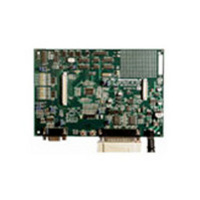
Manufacturer Part Number
MC56F8323EVME
Description
BOARD EVALUATION MC56F8323
Manufacturer
Freescale Semiconductor
Type
DSPr
Specifications of MC56F8323EVME
Contents
Module and Misc Hardware
Processor To Be Evaluated
MC56F8322 and MC56F8323
Data Bus Width
16 bit
Interface Type
RS-232
Silicon Manufacturer
Freescale
Core Architecture
56800/E
Core Sub-architecture
56800/E
Silicon Core Number
MC56F
Silicon Family Name
MC56F83xx
Rohs Compliant
Yes
For Use With/related Products
MC56F8322, MC56F8323
Lead Free Status / RoHS Status
Lead free / RoHS Compliant


20
Signal Name
OCR_DIS
(GPIOC0)
(GPIOC1)
EXTAL
V
V
V
V
XTAL
TCK
CAP
CAP
CAP
CAP
1
2
3
4
Table 2-2 Signal and Package Information for the 64-Pin LQFP
Pin No.
57
23
43
45
46
47
53
5
Schmitt
Schmitt
Schmitt
Supply
Output
Output
Output
Input/
Input/
Type
Input
Input
State During
pulled low
internally
Supply
Output
Reset
56F8323 Technical Data, Rev. 17
Input,
Input
V
connect each pin to a 2.2μF or greater bypass capacitor in order to
bypass the core logic voltage regulator, required for proper chip
operation.
When OCR_DIS is tied to V
become V
power supply.
Note: This bypass is required even if the chip is powered with
an external supply.
On-Chip Regulator Disable —
Tie this pin to V
Tie this pin to V
This pin is intended to be a static DC signal from power-up to
shut down. Do not try to toggle this pin for power savings
during operation.
External Crystal Oscillator Input — This input can be connected to
an 8MHz external crystal. If an external clock is used, XTAL must be
used as the input and EXTAL connected to V
The input clock can be selected to provide the clock directly to the
core. This input clock can also be selected as the input clock for the
on-chip PLL.
Port C GPIO — This GPIO pin can be individually programmed as
an input or output pin.
After reset, the default state is an EXTAL input with pull-ups disabled.
Crystal Oscillator Output — This output can be connected to an
8MHz external crystal. If an external clock is used, XTAL must be
used as the input and EXTAL connected to V
The input clock can be selected to provide the clock directly to the
core. This input clock can also be selected as the input clock for the
on-chip PLL.
Port C GPIO — This GPIO pin can be individually programmed as
an input or output pin.
After reset, the default state is an XTAL input with pull-ups disabled.
Test Clock Input — This input pin provides a gated clock to
synchronize the test logic and shift serial data to the JTAG/EOnCE
port. The pin is connected internally to a pull-down resistor. A Schmitt
trigger input is used for noise immunity.
CAP
1 - 4 — When OCR_DIS is tied to V
DD_CORE
SS
DD
to enable the on-chip regulator
to disable the on-chip regulator
and should be connected to a regulated 2.5V
Signal Description
DD
, (regulator disabled), these pins
SS
Freescale Semiconductor
(regulator enabled),
SS
SS
.
.
Preliminary
Related parts for MC56F8323EVME
Image
Part Number
Description
Manufacturer
Datasheet
Request
R

Part Number:
Description:
Manufacturer:
Freescale Semiconductor, Inc
Datasheet:
Part Number:
Description:
Manufacturer:
Freescale Semiconductor, Inc
Datasheet:
Part Number:
Description:
Manufacturer:
Freescale Semiconductor, Inc
Datasheet:
Part Number:
Description:
Manufacturer:
Freescale Semiconductor, Inc
Datasheet:
Part Number:
Description:
Manufacturer:
Freescale Semiconductor, Inc
Datasheet:
Part Number:
Description:
Manufacturer:
Freescale Semiconductor, Inc
Datasheet:
Part Number:
Description:
Manufacturer:
Freescale Semiconductor, Inc
Datasheet:
Part Number:
Description:
Manufacturer:
Freescale Semiconductor, Inc
Datasheet:
Part Number:
Description:
Manufacturer:
Freescale Semiconductor, Inc
Datasheet:
Part Number:
Description:
Manufacturer:
Freescale Semiconductor, Inc
Datasheet:
Part Number:
Description:
Manufacturer:
Freescale Semiconductor, Inc
Datasheet:
Part Number:
Description:
Manufacturer:
Freescale Semiconductor, Inc
Datasheet:
Part Number:
Description:
Manufacturer:
Freescale Semiconductor, Inc
Datasheet:
Part Number:
Description:
Manufacturer:
Freescale Semiconductor, Inc
Datasheet:
Part Number:
Description:
Manufacturer:
Freescale Semiconductor, Inc
Datasheet: