C8051F540-TB Silicon Laboratories Inc, C8051F540-TB Datasheet - Page 152
C8051F540-TB
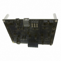
Manufacturer Part Number
C8051F540-TB
Description
BOARD PROTOTYPE W/C8051F540
Manufacturer
Silicon Laboratories Inc
Type
MCUr
Specifications of C8051F540-TB
Contents
Board
Processor To Be Evaluated
C8051F54x
Processor Series
C8051F54x
Interface Type
USB
Operating Supply Voltage
5 V
Lead Free Status / RoHS Status
Lead free / RoHS Compliant
For Use With/related Products
C8051F54x
Lead Free Status / Rohs Status
Lead free / RoHS Compliant
Other names
336-1672


C8051F54x
18.4. Port I/O Initialization
Port I/O initialization consists of the following steps:
1. Select the input mode (analog or digital) for all Port pins, using the Port Input Mode register (PnMDIN).
2. Select the output mode (open-drain or push-pull) for all Port pins, using the Port Output Mode register
3. Select any pins to be skipped by the I/O Crossbar using the Port Skip registers (PnSKIP).
4. Assign Port pins to desired peripherals.
5. Enable the Crossbar (XBARE = 1).
All Port pins must be configured as either analog or digital inputs. Any pins to be used as Comparator or
ADC inputs should be configured as an analog inputs. When a pin is configured as an analog input, its
weak pullup, digital driver, and digital receiver are disabled. This process saves power and reduces noise
on the analog input. Pins configured as digital inputs may still be used by analog peripherals; however this
practice is not recommended.
Additionally, all analog input pins should be configured to be skipped by the Crossbar (accomplished by
setting the associated bits in PnSKIP). Port input mode is set in the PnMDIN register, where a 1 indicates a
digital input, and a 0 indicates an analog input. All pins default to digital inputs on reset. See SFR Definition
18.13 for the PnMDIN register details.
152
(PnMDOUT).
Port
Special
Function
Signals
PIN I/O
UART_TX
UART_RX
SCK
MISO
MOSI
NSS
SDA
SCL
CP0
CP0A
CP1
CP1A
SYSCLK
CEX0
CEX1
CEX2
CEX3
CEX4
CEX5
ECI
T0
T1
LIN_TX
LIN_RX
Figure 18.4. Crossbar Priority Decoder in Example Configuration
0
0
1
1
2
1
P0SKIP[0:7]
3
0
P0
4
0
5
1
6
0
7
0
0
0
1
0
2
0
P1SKIP[0:7]
Rev. 1.1
*NSS Is only pinned out in 4-wire SPI Mode
3
0
P1
4
0
5
0
6
0
7
0
0
0
1
0
2
0
P2SKIP[0:7]
P2.2-P2.7, P3.0 only available on
3
0
P2
the 32-pin packages
4
0
5
0
6
0
7
0
P3SKIP[0]
P3
0
0
Related parts for C8051F540-TB
Image
Part Number
Description
Manufacturer
Datasheet
Request
R

Part Number:
Description:
SMD/C°/SINGLE-ENDED OUTPUT SILICON OSCILLATOR
Manufacturer:
Silicon Laboratories Inc
Part Number:
Description:
Manufacturer:
Silicon Laboratories Inc
Datasheet:
Part Number:
Description:
N/A N/A/SI4010 AES KEYFOB DEMO WITH LCD RX
Manufacturer:
Silicon Laboratories Inc
Datasheet:
Part Number:
Description:
N/A N/A/SI4010 SIMPLIFIED KEY FOB DEMO WITH LED RX
Manufacturer:
Silicon Laboratories Inc
Datasheet:
Part Number:
Description:
N/A/-40 TO 85 OC/EZLINK MODULE; F930/4432 HIGH BAND (REV E/B1)
Manufacturer:
Silicon Laboratories Inc
Part Number:
Description:
EZLink Module; F930/4432 Low Band (rev e/B1)
Manufacturer:
Silicon Laboratories Inc
Part Number:
Description:
I°/4460 10 DBM RADIO TEST CARD 434 MHZ
Manufacturer:
Silicon Laboratories Inc
Part Number:
Description:
I°/4461 14 DBM RADIO TEST CARD 868 MHZ
Manufacturer:
Silicon Laboratories Inc
Part Number:
Description:
I°/4463 20 DBM RFSWITCH RADIO TEST CARD 460 MHZ
Manufacturer:
Silicon Laboratories Inc
Part Number:
Description:
I°/4463 20 DBM RADIO TEST CARD 868 MHZ
Manufacturer:
Silicon Laboratories Inc
Part Number:
Description:
I°/4463 27 DBM RADIO TEST CARD 868 MHZ
Manufacturer:
Silicon Laboratories Inc
Part Number:
Description:
I°/4463 SKYWORKS 30 DBM RADIO TEST CARD 915 MHZ
Manufacturer:
Silicon Laboratories Inc
Part Number:
Description:
N/A N/A/-40 TO 85 OC/4463 RFMD 30 DBM RADIO TEST CARD 915 MHZ
Manufacturer:
Silicon Laboratories Inc
Part Number:
Description:
I°/4463 20 DBM RADIO TEST CARD 169 MHZ
Manufacturer:
Silicon Laboratories Inc