C8051F560-TB Silicon Laboratories Inc, C8051F560-TB Datasheet - Page 71
C8051F560-TB
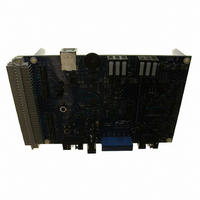
Manufacturer Part Number
C8051F560-TB
Description
BOARD PROTOTYPE W/C8051F560
Manufacturer
Silicon Laboratories Inc
Type
MCUr
Datasheet
1.TOOLSTICK560DC.pdf
(302 pages)
Specifications of C8051F560-TB
Contents
Board
Processor To Be Evaluated
C8051F56x
Processor Series
C8051F56x
Interface Type
USB
Maximum Operating Temperature
+ 125 C
Minimum Operating Temperature
- 40 C
Operating Supply Voltage
1.8 V to 5.25 V
Lead Free Status / RoHS Status
Lead free / RoHS Compliant
For Use With/related Products
C8051F55x, C8051F56x, C8051F57x
For Use With
336-1691 - KIT DEVELOPMENT FOR C8051F560
Lead Free Status / Rohs Status
Lead free / RoHS Compliant
Other names
336-1694


Comparator outputs can be polled in software, used as an interrupt source, and/or routed to a Port pin.
When routed to a Port pin, Comparator outputs are available asynchronous or synchronous to the system
clock; the asynchronous output is available even in STOP mode (with no system clock active). When dis-
abled, the Comparator output (if assigned to a Port I/O pin via the Crossbar) defaults to the logic low state,
and the power supply to the comparator is turned off. See Section “19.3. Priority Crossbar Decoder” on
page 170 for details on configuring Comparator outputs via the digital Crossbar. Comparator inputs can be
externally driven from –0.25 V to (V
trical specifications are given in Table 5.12.
The Comparator response time may be configured in software via the CPTnMD registers (see SFR Defini-
tion 8.2). Selecting a longer response time reduces the Comparator supply current. See Table 5.12 for
complete timing and supply current requirements.
Comparator hysteresis is software-programmable via its Comparator Control register CPTnCN.
The amount of negative hysteresis voltage is determined by the settings of the CPnHYN bits. As shown in
Figure 8.2, various levels of negative hysteresis can be programmed, or negative hysteresis can be dis-
abled. In a similar way, the amount of positive hysteresis is determined by the setting the CPnHYP bits.
Comparator interrupts can be generated on both rising-edge and falling-edge output transitions. (For Inter-
rupt enable and priority control, see “13. Interrupts” .) The CPnFIF flag is set to 1 upon a Comparator fall-
ing-edge, and the CPnRIF flag is set to 1 upon the Comparator rising-edge. Once set, these bits remain
set until cleared by software. The output state of the Comparator can be obtained at any time by reading
the CPnOUT bit. The Comparator is enabled by setting the CPnEN bit to 1, and is disabled by clearing this
bit to 0.
(Programmed with CPnHYP Bits)
Positive Hysteresis Voltage
INPUTS
OUTPUT
VIN+
VIN-
CIRCUIT CONFIGURATION
Positive Hysteresis
CPn-
VIN+
CPn+
VIN-
V
Disabled
OL
Figure 8.2. Comparator Hysteresis Plot
V
OH
+
_
CPn
DD
) + 0.25 V without damage or upset. The complete Comparator elec-
Positive Hysteresis
Maximum
OUT
Rev. 1.1
Negative Hysteresis
Disabled
C8051F55x/56x/57x
Negative Hysteresis
(Programmed by CPnHYN Bits)
Maximum
Negative Hysteresis Voltage
71
Related parts for C8051F560-TB
Image
Part Number
Description
Manufacturer
Datasheet
Request
R

Part Number:
Description:
SMD/C°/SINGLE-ENDED OUTPUT SILICON OSCILLATOR
Manufacturer:
Silicon Laboratories Inc
Part Number:
Description:
Manufacturer:
Silicon Laboratories Inc
Datasheet:
Part Number:
Description:
N/A N/A/SI4010 AES KEYFOB DEMO WITH LCD RX
Manufacturer:
Silicon Laboratories Inc
Datasheet:
Part Number:
Description:
N/A N/A/SI4010 SIMPLIFIED KEY FOB DEMO WITH LED RX
Manufacturer:
Silicon Laboratories Inc
Datasheet:
Part Number:
Description:
N/A/-40 TO 85 OC/EZLINK MODULE; F930/4432 HIGH BAND (REV E/B1)
Manufacturer:
Silicon Laboratories Inc
Part Number:
Description:
EZLink Module; F930/4432 Low Band (rev e/B1)
Manufacturer:
Silicon Laboratories Inc
Part Number:
Description:
I°/4460 10 DBM RADIO TEST CARD 434 MHZ
Manufacturer:
Silicon Laboratories Inc
Part Number:
Description:
I°/4461 14 DBM RADIO TEST CARD 868 MHZ
Manufacturer:
Silicon Laboratories Inc
Part Number:
Description:
I°/4463 20 DBM RFSWITCH RADIO TEST CARD 460 MHZ
Manufacturer:
Silicon Laboratories Inc
Part Number:
Description:
I°/4463 20 DBM RADIO TEST CARD 868 MHZ
Manufacturer:
Silicon Laboratories Inc
Part Number:
Description:
I°/4463 27 DBM RADIO TEST CARD 868 MHZ
Manufacturer:
Silicon Laboratories Inc
Part Number:
Description:
I°/4463 SKYWORKS 30 DBM RADIO TEST CARD 915 MHZ
Manufacturer:
Silicon Laboratories Inc
Part Number:
Description:
N/A N/A/-40 TO 85 OC/4463 RFMD 30 DBM RADIO TEST CARD 915 MHZ
Manufacturer:
Silicon Laboratories Inc
Part Number:
Description:
I°/4463 20 DBM RADIO TEST CARD 169 MHZ
Manufacturer:
Silicon Laboratories Inc